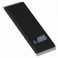
AT49BV040B-TU Atmel, AT49BV040B-TU Datasheet - Page 4

AT49BV040B-TU
Manufacturer Part Number
AT49BV040B-TU
Description
IC FLASH 4MBIT 70NS 32TSOP
Manufacturer
Atmel
Datasheet
1.AT49BV040B-JU.pdf
(21 pages)
Specifications of AT49BV040B-TU
Format - Memory
FLASH
Memory Type
FLASH
Memory Size
4M (512K x 8)
Speed
70ns
Interface
Parallel
Voltage - Supply
2.7 V ~ 3.6 V, 4.5 V ~ 5.5 V
Operating Temperature
-40°C ~ 85°C
Package / Case
32-TSOP
Lead Free Status / RoHS Status
Lead free / RoHS Compliant
Other names
AT49BV040B-70TU
AT49BV040B-70TU
AT49BV040B-70TU
Available stocks
Company
Part Number
Manufacturer
Quantity
Price
Company:
Part Number:
AT49BV040B-TU
Manufacturer:
ATMEL
Quantity:
4 000
Part Number:
AT49BV040B-TU
Manufacturer:
ATMEL/爱特梅尔
Quantity:
20 000
4.3
4.3.1
4.3.2
4.4
4.5
4
Erasure
Byte Programming
Boot Sector Programming Lockout
AT49BV040B
Chip Erase
Sector Erase
Before a byte can be reprogrammed, it must be erased. The erased state of memory bits is a
logical “1”. The entire device can be erased by using the Chip Erase command or individual sec-
tors can be erased by using the Sector Erase command.
If the boot block lockout has been enabled, the Chip Erase function will erase Parameter Sector
1, Parameter Sector 2, Main Memory Sectors 1 - 8, but not the boot sector. If the Boot Sector
Lockout has not been enabled, the Chip Erase function will erase the entire chip. After the full
chip erase the device will return back to read mode. Any command during chip erase will be
ignored.
As an alternative to a full chip erase, the device is organized into sectors that can be individually
erased. There are two 8K-byte parameter sectors and eight main memory sectors. The 8K-byte
parameter sectors and the eight main memory sectors can be independently erased and repro-
grammed. The Sector Erase command is a six bus cycle operation. The sector address is
latched on the falling WE edge of the sixth cycle while the 30H data input command is latched at
the rising edge of WE. The sector erase starts after the rising edge of WE of the sixth cycle. The
erase operation is internally controlled; it will automatically time to completion.
Once the memory array is erased, the device is programmed (to a logical “0”) on a byte-by-byte
basis. Please note that a data “0” cannot be programmed back to a “1”; only erase operations
can convert “0”s to “1”s. Programming is accomplished via the internal device command register
and is a 4-bus cycle operation (see
automatically generate the required internal program pulses.
The program cycle has addresses latched on the falling edge of WE or CE, whichever occurs
last, and the data latched on the rising edge of WE or CE, whichever occurs first. Programming
is completed after the specified t
be used to indicate the end of a program cycle.
The device has one designated sector that has a programming lockout feature. This feature pre-
vents programming of data in the designated sector once the feature has been enabled. The
size of the sector is 16K bytes. This sector, referred to as the boot sector, can contain secure
code that is used to bring up the system. Enabling the lockout feature will allow the boot code to
stay in the device while data in the rest of the device is updated. This feature does not have to
be activated; the boot sector’s usage as a write protected region is optional to the user. The
address range of the boot sector is 00000 to 03FFF.
Once the feature is enabled, the data in the boot sector can no longer be erased or pro-
grammed. Data in the main memory and parameter sectors can still be changed through the
regular programming method. To activate the lockout feature, a series of six program commands
to specific addresses with specific data must be performed. See
page
7.
BP
cycle time. The DATA polling or toggle bit feature may also
“Command Definition Table” on page
“Command Definition Table” on
7). The device will
3499B–FLASH–4/06


