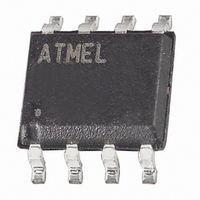
AT45DB161D-SU Atmel, AT45DB161D-SU Datasheet - Page 22

AT45DB161D-SU
Manufacturer Part Number
AT45DB161D-SU
Description
IC FLASH 16MBIT 66MHZ 8SOIC
Manufacturer
Atmel
Datasheets
1.AT45DB161D-CU.pdf
(51 pages)
2.AT45DB161D-SU.pdf
(6 pages)
3.AT45DB161D-SU.pdf
(53 pages)
Specifications of AT45DB161D-SU
Format - Memory
FLASH
Memory Type
DataFLASH
Memory Size
16M (4096 pages x 528 bytes)
Speed
66MHz
Interface
SPI, 3-Wire Serial
Voltage - Supply
2.7 V ~ 3.6 V
Operating Temperature
-40°C ~ 85°C
Package / Case
8-SOIC (5.3mm Width), 8-SOP, 8-SOEIAJ
Architecture
Sectored
Interface Type
SPI
Supply Voltage (max)
3.6 V
Supply Voltage (min)
2.7 V
Maximum Operating Current
15 mA
Mounting Style
SMD/SMT
Organization
128 KB x 16
Current, Input, Leakage
1 μA
Current, Operating
11 mA (Read), 12 mA (Program/Erase)
Current, Output, Leakage
1
Data Retention
20 yrs.
Density
16M
Package Type
EIAJ SOIC
Temperature, Operating
-40 to +85 °C
Time, Access
6 ns
Time, Address Hold
5
Time, Address Setup
5
Time, Fall
6.8 ns
Time, Rise
6.8 ns
Voltage, Input, High
1.89 to 2.52 V
Voltage, Input, Low
0.81 to 1.08 V
Voltage, Output, High
2.5 V
Voltage, Output, Low
0.4 V
Voltage, Supply
2.7 to 3.6 V
Memory Configuration
4096 Pages X 528 Bytes
Clock Frequency
66MHz
Supply Voltage Range
2.5V To 3.6V, 2.7V To 3.6V
Rohs Compliant
Yes
Access Time (max)
6ns
Boot Type
Not Required
Address Bus
1b
Operating Supply Voltage (typ)
3/3.3V
Operating Temp Range
-40C to 85C
Program/erase Volt (typ)
2.7 to 3.6V
Sync/async
Synchronous
Operating Temperature Classification
Industrial
Operating Supply Voltage (min)
2.7V
Operating Supply Voltage (max)
3.6V
Supply Current
15mA
Mounting
Surface Mount
Pin Count
8
Lead Free Status / RoHS Status
Lead free / RoHS Compliant
Available stocks
Company
Part Number
Manufacturer
Quantity
Price
Company:
Part Number:
AT45DB161D-SU
Manufacturer:
ATMEL
Quantity:
106 020
Company:
Part Number:
AT45DB161D-SU
Manufacturer:
AYMEL
Quantity:
1
Part Number:
AT45DB161D-SU
Manufacturer:
ATMEL/爱特梅尔
Quantity:
20 000
Part Number:
AT45DB161D-SU-2.5
Manufacturer:
ATMEL/爱特梅尔
Quantity:
20 000
Company:
Part Number:
AT45DB161D-SU-N03
Manufacturer:
NS
Quantity:
487
Company:
Part Number:
AT45DB161D-SU-SL383
Manufacturer:
AMS
Quantity:
30 000
11.2
11.3
22
Main Memory Page to Buffer Compare
Auto Page Rewrite
AT45DB161D
A page of data in main memory can be compared to the data in buffer 1 or buffer 2. To initiate
the operation for standard DataFlash page size, a 1-byte opcode, 60H for buffer 1 and 61H for
buffer 2, must be clocked into the device, followed by three address bytes consisting of 2 don’t
care bits, 12 page address bits (PA11 - PA0) that specify the page in the main memory that is to
be compared to the buffer, and 10 don’t care bits. To start a main memory page to buffer com-
pare for a binary page size, the opcode 60H for buffer 1 or 61H for buffer 2, must be clocked into
the device followed by three address bytes consisting of 3 don’t care bits, 12 page address bits
(A20 - A9) that specify the page in the main memory that is to be compared to the buffer, and 9
don’t care bits. The CS pin must be low while toggling the SCK pin to load the opcode and the
address bytes from the input pin (SI). On the low-to-high transition of the CS pin, the data bytes
in the selected main memory page will be compared with the data bytes in buffer 1 or buffer 2.
During this time (t
busy. On completion of the compare operation, bit 6 of the status register is updated with the
result of the compare.
This mode is only needed if multiple bytes within a page or multiple pages of data are modified in
a random fashion within a sector. This mode is a combination of two operations: Main Memory
Page to Buffer Transfer and Buffer to Main Memory Page Program with Built-in Erase. A page of
data is first transferred from the main memory to buffer 1 or buffer 2, and then the same data
(from buffer 1 or buffer 2) is programmed back into its original page of main memory. To start the
rewrite operation for standard DataFlash page size (528 bytes), a 1-byte opcode, 58H for buffer
1 or 59H for buffer 2, must be clocked into the device, followed by three address bytes com-
prised of 2 don’t care bits, 12 page address bits (PA11-PA0) that specify the page in main
memory to be rewritten and 10 don’t care bits. To initiate an auto page rewrite for a binary page
size (512 bytes), the opcode 58H for buffer 1 or 59H for buffer 2, must be clocked into the device
followed by three address bytes consisting of 3 don’t care bits, 12 page address bits (A20 - A9)
that specify the page in the main memory that is to be written and 9 don’t care bits. When a low-
to-high transition occurs on the CS pin, the part will first transfer data from the page in main
memory to a buffer and then program the data from the buffer back into same page of main
memory. The operation is internally self-timed and should take place in a maximum time of t
During this time, the status register and the RDY/BUSY pin will indicate that the part is busy.
If a sector is programmed or reprogrammed sequentially page by page, then the programming
algorithm shown in
page or several pages are programmed randomly in a sector, then the programming algorithm
shown in
updated/rewritten at least once within every 10,000 cumulative page erase/program operations
in that sector.
Figure 25-2 (page
COMP
Figure 25-1 (page
), the status register and the RDY/BUSY pin will indicate that the part is
46) is recommended. Each page within a sector must be
45) is recommended. Otherwise, if multiple bytes in a
3500I–DFLASH–8/07
EP
.


