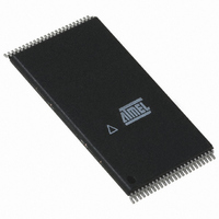
AT49BV4096A-90TC Atmel, AT49BV4096A-90TC Datasheet - Page 4

AT49BV4096A-90TC
Manufacturer Part Number
AT49BV4096A-90TC
Description
IC FLASH 4MBIT 90NS 48TSOP
Manufacturer
Atmel
Datasheet
1.AT49BV4096A-70TI.pdf
(16 pages)
Specifications of AT49BV4096A-90TC
Format - Memory
FLASH
Memory Type
FLASH
Memory Size
4M (512K x 8 or 256K x 16)
Speed
90ns
Interface
Parallel
Voltage - Supply
2.7 V ~ 3.6 V
Operating Temperature
0°C ~ 70°C
Package / Case
48-TSOP
Lead Free Status / RoHS Status
Contains lead / RoHS non-compliant
Available stocks
Company
Part Number
Manufacturer
Quantity
Price
Company:
Part Number:
AT49BV4096A-90TC
Manufacturer:
ATMEL
Quantity:
26
CHIP ERASE: The entire device can be erased at one time by using the 6-byte chip
erase software code. After the chip erase has been initiated, the device will internally
time the erase operation so that no external clocks are required. The maximum time to
erase the chip is t
.
EC
If the boot block lockout has been enabled, the chip erase will not erase the data in the
boot block; it will erase the main memory block and the parameter blocks only. After the
chip erase, the device will return to the read or standby mode.
SECTOR ERASE: As an alternative to a full chip erase, the device is organized into four
sectors that can be individually erased. There are two 4K word parameter block sec-
tions, one boot block, and the main memory array block. The Sector Erase command is
a six-bus cycle operation. The sector address is latched on the falling WE edge of the
sixth cycle while the 30H data input command is latched at the rising edge of WE. The
sector erase starts after the rising edge of WE of the sixth cycle. The erase operation is
internally controlled; it will automatically time to completion. Whenever the main memory
block is erased and reprogrammed, the two parameter blocks should be erased and
reprogrammed before the main memory block is erased again. Whenever a parameter
block is erased and reprogrammed, the other parameter block should be erased and
reprogrammed before the first parameter block is erased again. Whenever the boot
block is erased and reprogrammed, the main memory block and the parameter blocks
should be erased and reprogrammed before the boot block is erased again.
BYTE/WORD PROGRAMMING: Once a memory block is erased, it is programmed (to
a logic “0”) on a byte-by-byte or word-by-word basis. Programming is accomplished via
the internal device command register and is a four-bus cycle operation. The device will
automatically generate the required internal program pulses.
Any commands written to the chip during the embedded programming cycle will be
ignored. If a hardware reset happens during programming, the data at the location being
programmed will be corrupted. Please note that a data “0” cannot be programmed back
to a “1”; only erase operations can convert “0”s to “1”s. Programming is completed after
the specified t
cycle time. The Data Polling feature may also be used to indicate the
BP
end of a program cycle.
BOOT BLOCK PROGRAMMING LOCKOUT: The device has one designated block
that has a programming lockout feature. This feature prevents programming of data in
the designated block once the feature has been enabled. The size of the block is 8K
words. This block, referred to as the boot block, can contain secure code that is used to
bring up the system. Enabling the lockout feature will allow the boot code to stay in the
device while data in the rest of the device is updated. This feature does not have to be
activated; the boot block’s usage as a write-protected region is optional to the user. The
address range of the boot block is 00000H to 01FFFH.
Once the feature is enabled, the data in the boot block can no longer be erased or pro-
grammed when input levels of 5.5V or less are used. Data in the main memory block
can still be changed through the regular programming method. To activate the lockout
feature, a series of six program commands to specific addresses with specific data must
be performed. Please refer to the Command Definitions table.
BOOT BLOCK LOCKOUT DETECTION: A software method is available to determine if
programming of the boot block section is locked out. When the device is in the software
product identification mode (see Software Product Identification Entry and Exit sections)
a read from the following address location will show if programming the boot block is
locked out – 00002H. If the data on I/O0 is low, the boot block can be programmed; if
the data on I/O0 is high, the program lockout feature has been enabled and the block
AT49BV/LV4096A
4
1618H–FLASH–4/04


