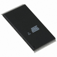
AT49BV4096A-90TC Atmel, AT49BV4096A-90TC Datasheet

AT49BV4096A-90TC
Specifications of AT49BV4096A-90TC
Available stocks
Related parts for AT49BV4096A-90TC
AT49BV4096A-90TC Summary of contents
Page 1
... A-1 (LSB Address Input, Byte Mode) BYTE Selects Byte or Word Mode NC No Connect 4-megabit (512K x 8/ 256K x 16) Single 2.7-volt ™ Battery-Voltage Flash Memory AT49BV4096A AT49LV4096A Not Recommended for New Design Contact Atmel to discuss the latest design in trends and options Rev. 1618H–FLASH–4/04 1 ...
Page 2
... The memory is divided into four blocks for erase opera- tions. There are two 4K word parameter block sections, the boot block, and the main memory array block. The typical number of program and erase cycles is in excess of 10,000 cycles. ...
Page 3
... Block Programming Lockout Override” section). ERASURE: Before a byte or word can be reprogrammed, it must be erased. The erased state of memory bits is a logic “1”. The entire device can be erased by using the Chip Erase command or individual sectors can be erased by using the Sector Erase commands ...
Page 4
... If the boot block lockout has been enabled, the chip erase will not erase the data in the boot block; it will erase the main memory block and the parameter blocks only. After the chip erase, the device will return to the read or standby mode. ...
Page 5
... TTL levels, the boot block programming lockout feature is again active. PRODUCT IDENTIFICATION: The product identification mode identifies the device and manufacturer as Atmel. It may be accessed by hardware or software operation. The hardware operation mode can be used by an external programmer to identify the correct programming algorithm for the Atmel product. For details, see “ ...
Page 6
... Either one of the Product ID Exit commands can be used sector addresses: (A17 - A0 01XXX for BOOT BLOCK SA = 02XXX for PARAMETER BLOCK 03XXX for PARAMETER BLOCK 3FXXX for MAIN MEMORY ARRAY Absolute Maximum Ratings* Temperature under Bias ................................ -55°C to +125°C Storage Temperature ..................................... -65°C to +150°C All Input Voltages (including NC Pins) with Respect to Ground ...
Page 7
... Condition MHz OUT -400 µA OH AT49BV/LV4096A AT49BV4096A-90 0°C - 70°C -40°C - 85°C 2.7V - 3. OUT High-Z High-Z X High-Z ( A17 = Manufacturer Code ( A17 = Device Code A17 = V Manufacturer Code A17 = V Device Code IH IL Min Max 10.0 10.0 50.0 0.5 25.0 0.6 2 ...
Page 8
... RO RESET HIGH Z OUTPUT OUTPUT - t after the address transition without impact on t ACC after the falling edge of CE without impact pF). L 2.4V 0. < 3.3V 1.8K OUTPUT PIN 1.3K 100 pF AT49BV4096A-90 Max Min Max 800 800 VALID . ACC after an address change CE ACC ...
Page 9
Pin Capacitance ( MHz 25°C Symbol Typ OUT Note: 1. This parameter is characterized and is not 100% tested. AC Word Load Characteristics Symbol Parameter Address, OE ...
Page 10
Program Cycle Characteristics Symbol Parameter t Byte/Word Programming Time BP t Address Setup Time AS t Address Hold Time AH t Data Setup Time DS t Data Hold Time DH t Write Pulse Width WP t Write Pulse Width High ...
Page 11
Data Polling Characteristics Symbol Parameter t Data Hold Time Hold Time OEH ( Output Delay OE t Write Recovery Time WR Notes: 1. These parameters are characterized and not 100% tested. 2. See t ...
Page 12
Software Product Identification Entry LOAD DATA AA TO ADDRESS 5555 LOAD DATA 55 TO ADDRESS 2AAA LOAD DATA 90 TO ADDRESS 5555 ENTER PRODUCT IDENTIFICATION (2)(3)(5) MODE Software Product Identification Exit OR LOAD DATA AA TO ADDRESS 5555 LOAD DATA ...
Page 13
... Wide, Plastic Gull Wing Small Outline (SOIC) 44R 48T 48-lead mm, Plastic Thin Small Outline Package (TSOP) 1618H–FLASH–4/04 Ordering Code AT49LV4096A-70TI AT49BV4096A-90RC AT49BV4096A-90TC AT49BV4096A-90TI Package Type AT49BV/LV4096A Package Operation Range 48T Industrial (-40° to 85°C) 44R Commercial 48T (0° ...
Page 14
Packaging Information 44R – SOIC Dimensions in Millimeters and (Inches). Controlling dimension: Inches. 2325 Orchard Parkway San Jose, CA 95131 R AT49BV/LV4096A 14 0.508(0.020) 0.356(0.014) 13.46(0.530) 13.21(0.520) PIN 1 1.27(0.050) BSC 28.32(1.115) 28.07(1.105) 0.33(0.130) 1.27(0.050) 0º ~ 8º 1.00(0.039) 0.60(0.024) ...
Page 15
TSOP Pin 1 Identifier e E Notes: 1. This package conforms to JEDEC reference MO-142, Variation DD. 2. Dimensions D1 and E do not include mold protrusion. Allowable protrusion 0.15 mm per side and on ...
Page 16
... No licenses to patents or other intellectual property of Atmel are granted by the Company in connection with the sale of Atmel products, expressly or by implication. Atmel’s products are not authorized for use as critical components in life support devices or systems. ...


