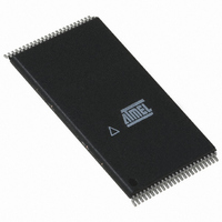
AT49BV161-90TI Atmel, AT49BV161-90TI Datasheet - Page 9

AT49BV161-90TI
Manufacturer Part Number
AT49BV161-90TI
Description
IC FLASH 16MBIT 90NS 48TSOP
Manufacturer
Atmel
Datasheet
1.AT49BV160-70CI.pdf
(29 pages)
Specifications of AT49BV161-90TI
Format - Memory
FLASH
Memory Type
FLASH
Memory Size
16M (2M x 8 or 1M x 16)
Speed
90ns
Interface
Parallel
Voltage - Supply
2.65 V ~ 3.3 V
Operating Temperature
-40°C ~ 85°C
Package / Case
48-TSOP
Lead Free Status / RoHS Status
Contains lead / RoHS non-compliant
AT49BV/LV160(T)/161(T)
RDY/BUSY: For the AT49BV/LV161(T), an open-drain READY/BUSY output pin provides
another method of detecting the end of a program or erase operation. RDY/BUSY is actively
pulled low during the internal program and erase cycles and is released at the completion of
the cycle. The open-drain connection allows for OR-tying of several devices to the same
RDY/BUSY line. Please see “Status Bit Table” on page 12 for more details.
HARDWARE DATA PROTECTION: The Hardware Data Protection feature protects against
inadvertent programs to the AT49BV/LV16X(T) in the following ways: (a) V
sense: if V
is
CC
CC
below 1.8V (typical), the program function is inhibited. (b) V
power-on delay: once V
has
CC
CC
reached the V
sense level, the device will automatically time out 10 ms (typical) before pro-
CC
gramming. (c) Program inhibit: holding any one of OE low, CE high or WE high inhibits
program cycles. (d) Noise filter: pulses of less than 15 ns (typical) on the WE or CE inputs will
not initiate a program cycle. (e) Program inhibit: V
is less than V
. (f) V
power-on delay:
PP
ILPP
PP
once V
has reached 1.65V, program and erase operations can occur after 100 ns.
PP
INPUT LEVELS: While operating with a 2.65V to 3.6V power supply, the address inputs and
control inputs (OE, CE and WE) may be driven from 0 to 5.5V without adversely affecting the
operation of the device. The I/O lines can only be driven from 0 to V
+ 0.6V.
CC
OUTPUT LEVELS: For the AT49BV/LV160(T), output high levels (V
) are equal to V
-
OH
CCQ
0.2V (not V
). For 2.65V - 3.6V output levels, V
must be tied to V
. For 1.8V - 2.2V out-
CC
CCQ
CC
put levels, V
must be regulated to 2.0V ± 10%, while V
must be regulated to 2.65V - 3.0V
CCQ
CC
(for minimum power).
9
1427L–FLASH–02/03


