AT45DB081B-TC-2.5 Atmel, AT45DB081B-TC-2.5 Datasheet - Page 4
AT45DB081B-TC-2.5
Manufacturer Part Number
AT45DB081B-TC-2.5
Description
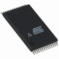
IC FLASH 8MBIT 20MHZ 28TSOP
Manufacturer
Atmel
Datasheet
1.AT45DB081B-CC.pdf
(33 pages)
Specifications of AT45DB081B-TC-2.5
Format - Memory
FLASH
Memory Type
DataFLASH
Memory Size
8M (4096 pages x 264 bytes)
Speed
20MHz
Interface
SPI, 3-Wire Serial
Voltage - Supply
2.5 V ~ 3.6 V
Operating Temperature
0°C ~ 70°C
Package / Case
28-TSOP
Lead Free Status / RoHS Status
Contains lead / RoHS non-compliant


downward compatibility to larger and smaller density devices (see Notes under “Command
Sequence for Read/Write Operations” diagram). The next 12 address bits (PA11 - PA0) specify
which page of the main memory array to read, and the last nine bits (BA8 - BA0) of the 24-bit
address sequence specify the starting byte address within the page. The 32 don’t care bits that
follow the 24 address bits are needed to initialize the read operation. Following the 32 don’t care
bits, additional clock pulses on the SCK pin will result in serial data being output on the SO
(serial output) pin.
The CS pin must remain low during the loading of the opcode, the address bits, the don’t care
bits, and the reading of data. When the end of a page in main memory is reached during a Con-
tinuous Array Read, the device will continue reading at the beginning of the next page with no
delays incurred during the page boundary crossover (the crossover from the end of one page to
the beginning of the next page). When the last bit in the main memory array has been read, the
device will continue reading back at the beginning of the first page of memory. As with crossing
over page boundaries, no delays will be incurred when wrapping around from the end of the
array to the beginning of the array.
A low-to-high transition on the CS pin will terminate the read operation and tri-state the SO pin.
The maximum SCK frequency allowable for the Continuous Array Read is defined by the f
CAR
specification. The Continuous Array Read bypasses both data buffers and leaves the contents
of the buffers unchanged.
MAIN MEMORY PAGE READ: A Main Memory Page Read allows the user to read data directly
from any one of the 4096 pages in the main memory, bypassing both of the data buffers and
leaving the contents of the buffers unchanged. To start a page read, an opcode of 52H or D2H
must be clocked into the device followed by 24 address bits and 32 don’t care bits. The first
three bits of the 24-bit address sequence are reserved bits, the next 12 address bits (PA11 -
PA0) specify the page address, and the next nine address bits (BA8 - BA0) specify the starting
byte address within the page. The 32 don’t care bits which follow the 24 address bits are sent to
initialize the read operation. Following the 32 don’t care bits, additional pulses on SCK result in
serial data being output on the SO (serial output) pin. The CS pin must remain low during the
loading of the opcode, the address bits, the don’t care bits, and the reading of data. When the
end of a page in main memory is reached during a Main Memory Page Read, the device will
continue reading at the beginning of the same page. A low-to-high transition on the CS pin will
terminate the read operation and tri-state the SO pin.
BUFFER READ: Data can be read from either one of the two buffers, using different opcodes to
specify which buffer to read from. An opcode of 54H or D4H is used to read data from buffer 1,
and an opcode of 56H or D6H is used to read data from buffer 2. To perform a Buffer Read, the
eight bits of the opcode must be followed by 15 don’t care bits, nine address bits, and eight don’t
care bits. Since the buffer size is 264 bytes, nine address bits (BFA8 - BFA0) are required to
specify the first byte of data to be read from the buffer. The CS pin must remain low during the
loading of the opcode, the address bits, the don’t care bits, and the reading of data. When the
end of a buffer is reached, the device will continue reading back at the beginning of the buffer. A
low-to-high transition on the CS pin will terminate the read operation and tri-state the SO pin.
STATUS REGISTER READ: The status register can be used to determine the device’s
Ready/Busy status, the result of a Main Memory Page to Buffer Compare operation, or the
device density. To read the status register, an opcode of 57H or D7H must be loaded into the
device. After the last bit of the opcode is shifted in, the eight bits of the status register, starting
with the MSB (bit 7), will be shifted out on the SO pin during the next eight clock cycles. The five
most significant bits of the status register will contain device information, while the remaining
three least-significant bits are reserved for future use and will have undefined values. After bit 0
of the status register has been shifted out, the sequence will repeat itself (as long as CS remains
AT45DB081B
4
2225J–DFLSH–2/08
Related parts for AT45DB081B-TC-2.5
Image
Part Number
Description
Manufacturer
Datasheet
Request
R

Part Number:
Description:
Manufacturer:
ATMEL Corporation
Datasheet:

Part Number:
Description:
IC FLASH 8MBIT 20MHZ 14CBGA
Manufacturer:
Atmel
Datasheet:
Part Number:
Description:
IC FLASH 8MBIT 20MHZ 14CBGA
Manufacturer:
Atmel
Datasheet:

Part Number:
Description:
IC FLASH 8MBIT 20MHZ 28TSOP
Manufacturer:
Atmel
Datasheet:

Part Number:
Description:
IC FLASH 8MBIT 20MHZ 8CASON
Manufacturer:
Atmel
Datasheet:
Part Number:
Description:
IC FLASH 8MBIT 20MHZ 8CASON
Manufacturer:
Atmel
Datasheet: