DS1251WP-120 Maxim Integrated Products, DS1251WP-120 Datasheet - Page 5
DS1251WP-120
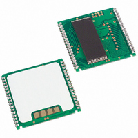
Manufacturer Part Number
DS1251WP-120
Description
IC NVSRAM 4MBIT 120NS 34PCM
Manufacturer
Maxim Integrated Products
Datasheet
1.DS1251Y-70.pdf
(21 pages)
Specifications of DS1251WP-120
Format - Memory
RAM
Memory Type
NVSRAM (Non-Volatile SRAM)
Memory Size
4M (512K x 8)
Speed
120ns
Interface
Parallel
Voltage - Supply
3 V ~ 3.6 V
Operating Temperature
0°C ~ 70°C
Package / Case
34-PowerCap™ Module
Lead Free Status / RoHS Status
Contains lead / RoHS non-compliant


from the timekeeping registers can proceed. The next 64 cycles will cause the
receive or transmit data on DQ0, depending on the level of th
locations outside the memory block can be interleaved with
re
PHANTOM CLOCK REGISTER INFORMATION
The phantom clock information is contained in eight registers of 8 bits, each of which is sequentially
accessed 1 bit at a time after the 64-bit pattern recognition sequence has been completed. When updating
the phantom clock registers, each register must be handled in groups of 8 bits. Writing and reading
individual
F
Data contained in the phantom clock register is in binary-coded decimal format (BCD). Reading and
writing the registers is always accomplished
re
P
igure 2.
cognition sequence or data transfer sequence to the phantom clock.
gister 0 and ending with bit 7 of register 7.
HANTOM CLOCK REGISTER DEFINITION Figure 1
NOTE: THE PATTERN RECOGNITION IN HEX IS C5, 3A, A3, 5C, C5, 3A, A3, 5C. THE ODDS OF THIS PATTERN BEING ACCIDENTALLY
DUPLICATED AND CAUSING INADVERTENT ENTRY TO THE PHANTOM CLOCK IS LESS THAN 1 IN 10
THE PHANTOM CLOCK LSB TO MSB.
bits within a register could produce erroneous results. These read/write registers are defined in
by stepping through all eight registers, starting with bit 0 of
5 of 21
CE
e
OE
cycles without interrupting the pattern
pin or the
19
. THIS PATTERN IS SENT TO
WE
pha
ntom clock to either
pin. Cycles to other
Related parts for DS1251WP-120
Image
Part Number
Description
Manufacturer
Datasheet
Request
R

Part Number:
Description:
IC NVSRAM 4MBIT 120NS 34PCM
Manufacturer:
Maxim Integrated Products
Datasheet:
Part Number:
Description:
IC NVSRAM 4MBIT 120NS 34PCM
Manufacturer:
Maxim Integrated Products
Datasheet:
Part Number:
Description:
IC NVSRAM 4MBIT 120NS 34PCM
Manufacturer:
Maxim Integrated Products
Datasheet:

Part Number:
Description:
IC NVSRAM 4MBIT 120NS 32DIP
Manufacturer:
Maxim Integrated Products
Datasheet:
Part Number:
Description:
IC NVSRAM 4MBIT 120NS 32DIP
Manufacturer:
Maxim Integrated Products
Datasheet:
Part Number:
Description:
IC NVSRAM 4MBIT 120NS 32DIP
Manufacturer:
Maxim Integrated Products
Datasheet:
Part Number:
Description:
IC NVSRAM 4MBIT 120NS 32DIP
Manufacturer:
Maxim Integrated Products
Datasheet:

Part Number:
Description:
CRANK HANDLE ROUND KNOB, 6.35MM
Manufacturer:
EHC (ELECTRONIC HARDWARE)


Part Number:
Description:
MAX7528KCWPMaxim Integrated Products [CMOS Dual 8-Bit Buffered Multiplying DACs]
Manufacturer:
Maxim Integrated Products
Datasheet:
Part Number:
Description:
Single +5V, fully integrated, 1.25Gbps laser diode driver.
Manufacturer:
Maxim Integrated Products
Datasheet:
Part Number:
Description:
Single +5V, fully integrated, 155Mbps laser diode driver.
Manufacturer:
Maxim Integrated Products
Datasheet: