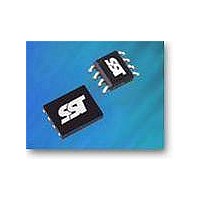
SST25VF512A-33-4C-QAE Microchip Technology, SST25VF512A-33-4C-QAE Datasheet - Page 6

SST25VF512A-33-4C-QAE
Manufacturer Part Number
SST25VF512A-33-4C-QAE
Description
IC FLASH SER 512K 33MHZ 8WSON
Manufacturer
Microchip Technology
Specifications of SST25VF512A-33-4C-QAE
Memory Type
FLASH
Memory Size
512K (64K x 8)
Operating Temperature
0°C ~ 70°C
Package / Case
8-WSON
Format - Memory
FLASH
Speed
33MHz
Interface
SPI Serial
Voltage - Supply
2.7 V ~ 3.6 V
Architecture
Sectored
Interface Type
4-Wire
Supply Voltage (max)
3.6 V
Supply Voltage (min)
2.7 V
Maximum Operating Current
10 mA
Mounting Style
SMD/SMT
Organization
4 KB x 16
Lead Free Status / RoHS Status
Lead free / RoHS Compliant
Lead Free Status / RoHS Status
Lead free / RoHS Compliant, Lead free / RoHS Compliant
Data Sheet
Status Register
The software status register provides status on whether the
flash memory array is available for any Read or Write oper-
ation, whether the device is Write enabled, and the state of
the memory Write protection. During an internal Erase or
TABLE 4: S
Busy
The Busy bit determines whether there is an internal Erase
or Program operation in progress. A “1” for the Busy bit indi-
cates the device is busy with an operation in progress. A “0”
indicates the device is ready for the next valid operation.
Write Enable Latch (WEL)
The Write-Enable-Latch bit indicates the status of the inter-
nal memory Write Enable Latch. If the Write-Enable-Latch
bit is set to “1”, it indicates the device is Write enabled. If the
bit is set to “0” (reset), it indicates the device is not Write
enabled and does not accept any memory Write (Program/
Erase) commands. The Write-Enable-Latch bit is automati-
cally reset under the following conditions:
•
•
•
•
•
•
•
©2006 Silicon Storage Technology, Inc.
4:5
Bit
0
1
2
3
6
7
Power-up
Write-Disable (WRDI) instruction completion
Byte-Program instruction completion
Auto Address Increment (AAI) programming
reached its highest memory address
Sector-Erase instruction completion
Block-Erase instruction completion
Chip-Erase instruction completion
Name
BUSY
WEL
RES
BP0
BP1
BPL
AAI
OFTWARE
Function
1 = Internal Write operation is in progress
0 = No internal Write operation is in progress
1 = Device is memory Write enabled
0 = Device is not memory Write enabled
Indicate current level of block write protection (See Table 5)
Indicate current level of block write protection (See Table 5)
Reserved for future use
Auto Address Increment Programming status
1 = AAI programming mode
0 = Byte-Program mode
1 = BP1, BP0 are read-only bits
0 = BP1, BP0 are read/writable
S
TATUS
R
EGISTER
6
Program operation, the status register may be read only to
determine the completion of an operation in progress.
Table 4 describes the function of each bit in the software
status register.
512 Kbit SPI Serial Flash
Default at
Power-up
0
0
1
1
0
0
0
SST25VF512A
S71264-02-000
Read/Write
R/W
R/W
R/W
N/A
R
R
R
T4.0 1264
1/06


