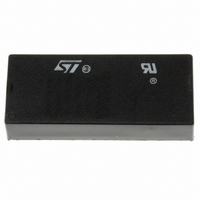
M48Z128Y-70PM1 STMicroelectronics, M48Z128Y-70PM1 Datasheet - Page 10

M48Z128Y-70PM1
Manufacturer Part Number
M48Z128Y-70PM1
Description
IC NVSRAM 1MBIT 70NS 32DIP
Manufacturer
STMicroelectronics
Type
NVSRAMr
Specifications of M48Z128Y-70PM1
Format - Memory
RAM
Memory Type
NVSRAM (Non-Volatile SRAM)
Memory Size
1M (128K x 8)
Speed
70ns
Interface
Parallel
Voltage - Supply
4.5 V ~ 5.5 V
Operating Temperature
0°C ~ 70°C
Package / Case
32-DIP (600 mil) Module
Data Bus Width
8 bit
Organization
128 Kb x 8
Interface Type
Parallel
Access Time
70 ns
Supply Voltage (max)
5.5 V
Supply Voltage (min)
4.5 V
Operating Current
105 mA
Maximum Operating Temperature
70 C
Minimum Operating Temperature
0 C
Mounting Style
Through Hole
Word Size
8b
Density
1Mb
Access Time (max)
70ns
Operating Supply Voltage (typ)
5V
Package Type
PMDIP
Operating Temperature Classification
Commercial
Operating Supply Voltage (max)
5.5V
Operating Supply Voltage (min)
4.5V
Operating Temp Range
0C to 70C
Pin Count
32
Mounting
Through Hole
Supply Current
105mA
Memory Configuration
128K X 8
Nvram Features
Internal Battery
Supply Voltage Range
4.5V To 5.5V
Memory Case Style
PMDIP
No. Of Pins
32
Rohs Compliant
Yes
Lead Free Status / RoHS Status
Lead free / RoHS Compliant
Other names
497-2874-5
Available stocks
Company
Part Number
Manufacturer
Quantity
Price
Part Number:
M48Z128Y-70PM1
Manufacturer:
ST
Quantity:
20 000
Operating modes
Table 4.
1. Valid for ambient operating temperature: T
2. C
3. If E goes low simultaneously with W going low, the outputs remain in the high impedance state.
2.3
10/20
t
t
WHQX
WLQZ
Symbol
t
noted).
t
t
t
t
t
t
t
t
t
t
t
t
WLWH
WHDX
WHAX
DVWH
AVWH
AVWL
EHDX
ELEH
EHAX
DVEH
AVEH
AVEL
AVAV
L
= 5 pF.
(2)(3)
(2)(3)
WRITE cycle time
Address valid to WRITE enable Low
Address valid to chip enable low
WRITE enable pulse width
Chip enable low to chip enable high
WRITE enable high to address transition
Chip enable high to address transition
Input valid to WRITE enable high
Input valid to chip enable high
WRITE enable high to input transition
Chip enable high to input transition
WRITE enable low to output Hi-Z
Address valid to WRITE enable high
Address valid to chip enable high
WRITE enable high to output transition
WRITE mode AC characteristics
Data retention mode
With valid V
RAM. Should the supply voltage decay, the RAM will automatically power-fail deselect, write
protecting itself t
inputs are treated as “Don't care.”
If power fail detection occurs during a valid access, the memory cycle continues to
completion. If the memory cycle fails to terminate within the time t
place. When V
source which preserves data.
The internal coin cell will maintain data in the M48Z128/Y/V after the initial application of
V
power returns and V
is switched to external V
allow for processor stabilization. After t
For more information on battery storage life refer to the application note AN1012.
CC
for an accumulated period of at least 10 years when V
CC
Parameter
CC
applied, the M48Z128/Y/V operates as a conventional BYTEWIDE
WP
drops below V
after V
CC
rises above V
(1)
CC
A
= 0 to 70 °C; V
CC
. Write protection continues for t
falls below V
Doc ID 2426 Rev 5
SO
, the control circuit switches power to the internal energy
SO
CC
ER
, the battery is disconnected, and the power supply
= 4.75 to 5.5 V, 4.5 to 5.5 V or 3.0 to 3.6 V (except where
, normal RAM operation can resume.
M48Z128/Y
PFD
Min
70
55
55
15
30
30
10
65
65
0
0
5
0
5
. All outputs become high impedance, and all
–70
Max
25
M48Z128/Y/V
Min
85
65
75
15
35
35
10
75
75
M48Z128, M48Z128Y, M48Z128V
0
0
5
0
5
CC
ER
–85
is less than V
after V
Max
30
WP
, write protection takes
CC
M48Z128/Y/V
reaches V
Min
120
100
100
100
85
15
45
45
10
0
0
5
0
5
–120
SO
. As system
Max
40
™
PFD
static
Unit
to
ns
ns
ns
ns
ns
ns
ns
ns
ns
ns
ns
ns
ns
ns
ns


