M48Z18-100PC1 STMicroelectronics, M48Z18-100PC1 Datasheet - Page 3
M48Z18-100PC1
Manufacturer Part Number
M48Z18-100PC1
Description
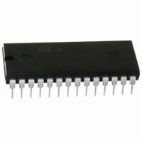
IC NVSRAM 64KBIT 100NS 28DIP
Manufacturer
STMicroelectronics
Specifications of M48Z18-100PC1
Format - Memory
RAM
Memory Type
NVSRAM (Non-Volatile SRAM)
Memory Size
64K (8K x 8)
Speed
100ns
Interface
Parallel
Voltage - Supply
4.5 V ~ 5.5 V
Operating Temperature
0°C ~ 70°C
Package / Case
28-DIP Module (600 mil), 28-EDIP
Data Bus Width
8 bit
Organization
8 Kb x 8
Interface Type
Parallel
Access Time
100 ns
Supply Voltage (max)
5.5 V
Supply Voltage (min)
4.5 V
Operating Current
80 mA
Maximum Operating Temperature
70 C
Minimum Operating Temperature
0 C
Mounting Style
Through Hole
Capacitance, Input
10 pF
Capacitance, Output
10 pF
Current, Input, Leakage
±1 μA
Current, Operating
80 mA
Current, Output, Leakage
±1
Data Retention
11 yrs.
Density
64K
Package Type
PCDIP28
Power Dissipation
1 W
Temperature, Operating
0 to +70 °C
Time, Access
100 ns
Time, Fall
≤5 ns
Time, Rise
≤5 ns
Voltage, Input, High
4.8 to 5.8 V
Voltage, Input, Low
0.8 V
Voltage, Output, High
2.4 V
Voltage, Output, Low
0.4 V
Voltage, Supply
4.5 to 5.5 V
Lead Free Status / RoHS Status
Lead free / RoHS Compliant
Other names
497-2877-5
Available stocks
Company
Part Number
Manufacturer
Quantity
Price
Company:

Part Number:
M48Z18-100PC1
Manufacturer:
ALCO
Quantity:
3 000
Part Number:
M48Z18-100PC1
Manufacturer:
ST
Quantity:
20 000


READ Mode
The M48Z08/18 is in the READ Mode whenever W
(WRITE Enable) is high and E (Chip Enable) is
low. The device architecture allows ripple-through
access of data from eight of 65,536 locations in the
static storage array. Thus, the unique address
specified by the 13 address inputs defines which
one of the 8,192 bytes of data is to be accessed.
Valid data will be available at the Data I/O pins
within address access time (t
address input signal is stable, providing that the E
and G access times are also satisfied. If the E and
G access times are not met, valid data will be
Figure 5. READ Mode AC Waveforms
Note: WRITE Enable (W) = High.
Table 3. READ Mode AC Characteristics
Note: 1. Valid for Ambient Operating Temperature: T
Symbol
t
t
t
t
GHQZ
GLQX
EHQZ
ELQX
t
t
t
t
t
GLQV
AXQX
2. C
AVQV
ELQV
AVAV
(2)
(2)
(2)
L
(2)
= 30pF.
A0-A12
E
G
DQ0-DQ7
READ Cycle Time
Address Valid to Output Valid
Chip Enable Low to Output Valid
Output Enable Low to Output Valid
Chip Enable Low to Output Transition
Output Enable Low to Output Transition
Chip Enable High to Output Hi-Z
Output Enable High to Output Hi-Z
Address Transition to Output Transition
Parameter
AVQV
) after the last
tAVQV
tELQX
(1)
tELQV
tGLQX
A
= 0 to 70°C; V
tGLQV
tAVAV
VALID
CC
available after the latter of the Chip Enable Access
time (t
(t
The state of the eight three-state Data I/O signals
is controlled by E and G. If the outputs are activat-
ed before t
indeterminate state until t
puts are changed while E and G remain active,
output data will remain valid for Output Data Hold
time (t
address access.
= 4.75 to 5.5V or 4.5 to 5.5V (except where noted).
GLQV
AXQX
).
ELQV
Min
100
10
5
5
M48Z08/M48Z18
AVQV
) but will go indeterminate until the next
VALID
) or Output Enable Access time
, the data lines will be driven to an
tGHQZ
Max
100
100
50
50
40
AVQV
M48Z08, M48Z18
. If the address in-
tAXQX
tEHQZ
AI01385
Unit
ns
ns
ns
ns
ns
ns
ns
ns
ns
5/16
Related parts for M48Z18-100PC1
Image
Part Number
Description
Manufacturer
Datasheet
Request
R

Part Number:
Description:
Manufacturer:
STMicroelectronics
Datasheet:
Part Number:
Description:
5v, 64 Kbit 8kb X 8 Zeropower Sram
Manufacturer:
STMicroelectronics
Datasheet:
Part Number:
Description:
STMicroelectronics [RIPPLE-CARRY BINARY COUNTER/DIVIDERS]
Manufacturer:
STMicroelectronics
Datasheet:
Part Number:
Description:
STMicroelectronics [LIQUID-CRYSTAL DISPLAY DRIVERS]
Manufacturer:
STMicroelectronics
Datasheet:

Part Number:
Description:
BOARD EVAL FOR MEMS SENSORS
Manufacturer:
STMicroelectronics
Datasheet:
Part Number:
Description:
NPN TRANSISTOR POWER MODULE
Manufacturer:
STMicroelectronics
Datasheet:
Part Number:
Description:
TURBOSWITCH ULTRA-FAST HIGH VOLTAGE DIODE
Manufacturer:
STMicroelectronics
Datasheet:
Part Number:
Description:
Manufacturer:
STMicroelectronics
Datasheet:
Part Number:
Description:
DIODE / SCR MODULE
Manufacturer:
STMicroelectronics
Datasheet:
Part Number:
Description:
DIODE / SCR MODULE
Manufacturer:
STMicroelectronics
Datasheet:
Part Number:
Description:
Search -----> STE16N100
Manufacturer:
STMicroelectronics
Datasheet: