CY7C1049DV33-10VXIT Cypress Semiconductor Corp, CY7C1049DV33-10VXIT Datasheet - Page 3
CY7C1049DV33-10VXIT
Manufacturer Part Number
CY7C1049DV33-10VXIT
Description
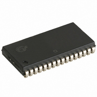
IC SRAM 4MBIT 10NS 36-SOJ
Manufacturer
Cypress Semiconductor Corp
Type
Asynchronousr
Specifications of CY7C1049DV33-10VXIT
Memory Size
4M (512K x 8)
Package / Case
36-SOJ
Format - Memory
RAM
Memory Type
SRAM - Asynchronous
Speed
10ns
Interface
Parallel
Voltage - Supply
3 V ~ 3.6 V
Operating Temperature
-40°C ~ 85°C
Access Time
10 ns
Supply Voltage (max)
3.6 V
Supply Voltage (min)
3 V
Maximum Operating Current
90 mA
Maximum Operating Temperature
+ 85 C
Minimum Operating Temperature
- 40 C
Mounting Style
SMD/SMT
Number Of Ports
1
Operating Supply Voltage
3.3 V
Memory Configuration
512K X 8
Supply Voltage Range
3V To 3.6V
Memory Case Style
SOJ
No. Of Pins
36
Operating Temperature Range
-40°C To +85°C
Lead Free Status / RoHS Status
Lead free / RoHS Compliant
Lead Free Status / RoHS Status
Lead free / RoHS Compliant, Lead free / RoHS Compliant
Available stocks
Company
Part Number
Manufacturer
Quantity
Price
Company:

Part Number:
CY7C1049DV33-10VXIT
Manufacturer:
CYPRESS
Quantity:
2 100
Company:
Part Number:
CY7C1049DV33-10VXIT
Manufacturer:
CY
Quantity:
6 250
Company:
Part Number:
CY7C1049DV33-10VXIT
Manufacturer:
CYPRESS/PBF
Quantity:
146
Part Number:
CY7C1049DV33-10VXIT
Manufacturer:
专营CYPRESS
Quantity:
20 000


Maximum Ratings
Exceeding the maximum ratings may impair the useful life of the
device. User guidelines are not tested.
Storage Temperature ................................. –65C to +150C
Ambient Temperature with
Power Applied ............................................ –55C to +125C
Supply Voltage on V
DC Voltage Applied to Outputs
in High Z State
DC Input Voltage
Electrical Characteristics
Capacitance
Tested initially and after any design or process changes that may affect these parameters.
Note
Document Number: 38-05475 Rev. *F
V
V
V
V
I
I
I
I
I
C
C
2. V
IX
OZ
CC
SB1
SB2
Parameter
Parameter
OH
OL
IH
IL
IN
OUT
[2]
[2]
IL
(min.) = –2.0V and V
Output HIGH Voltage
Output LOW Voltage
Input HIGH Voltage
Input LOW Voltage
Input Leakage Current
Output Leakage
Current
V
Supply Current
Automatic CE
Power down Current
—TTL Inputs
Automatic CE
Power down Current
—CMOS Inputs
Input Capacitance
IO Capacitance
[2]
CC
.................................... –0.3V to V
[2]
Operating
................................ –0.3V to V
CC
Description
IH
(max) = V
to Relative GND
Description
CC
[2]
+ 2V for pulse durations of less than 20 ns.
Over the Operating Range
[2]
GND < V
V
I
V
GND < V
Output Disabled
V
Max V
V
V
Max V
V
or V
OH
.....–0.3V to +4.6V
CC
CC
CC
IN
IN
IN
= –4.0 mA
> V
< V
> V
IN
= Max, f = f
= Min,
= Min, I
CC
CC
< 0.3V, f = 0
IH
IL
CC
, f = f
, CE > V
, CE > V
I
OUT
CC
CC
or
Test Conditions
< V
– 0.3V,
OL
+ 0.3V
+ 0.3V
< V
CC
MAX
MAX
= 8.0 mA
CC
T
IH
CC
A
= 1/t
;
,
= 25C, f = 1 MHz, V
– 0.3V,
RC
Test Conditions
Current into Outputs (LOW)......................................... 20 mA
Static Discharge Voltage............. ...............................>2001V
(MIL-STD-883, Method 3015)
Latch up Current...................................................... >200 mA
Operating Range
Industrial
Automotive
100 MHz
83 MHz
66 MHz
40 MHz
Range
CC
–0.3
Min
2.4
2.0
–1
–1
-10 (Industrial)
= 3.3V
–40C to +125C
–40C to +85C
Temperature
V
Ambient
CC
Max
0.4
0.8
+1
+1
90
80
70
60
20
10
+ 0.3
–0.3
Min
CY7C1049DV33
2.4
2.0
–1
–1
-12 (Automotive)
Max
3.3V 0.3V
3.3V 0.3V
8
8
V
V
CC
CC
Max
0.4
0.8
+1
+1
95
85
75
25
15
-
+ 0.3
Page 3 of 11
Unit
Speed
pF
pF
10 ns
12 ns
Unit
mA
mA
mA
mA
mA
mA
A
A
V
V
V
V
[+] Feedback
Related parts for CY7C1049DV33-10VXIT
Image
Part Number
Description
Manufacturer
Datasheet
Request
R

Part Number:
Description:
17ns, 512Kx8 static RAM (SRAM)
Manufacturer:
Cypress Semiconductor Corporation.
Datasheet:
Part Number:
Description:
20ns, 512Kx8 static RAM (SRAM)
Manufacturer:
Cypress Semiconductor Corporation.
Datasheet:
Part Number:
Description:
20ns, 512Kx8 static RAM (SRAM)
Manufacturer:
Cypress Semiconductor Corporation.
Datasheet:
Part Number:
Description:
15ns, 512Kx8 static RAM (SRAM)
Manufacturer:
Cypress Semiconductor Corporation.
Datasheet:
Part Number:
Description:
25ns, 512Kx8 static RAM (SRAM)
Manufacturer:
Cypress Semiconductor Corporation.
Datasheet:

Part Number:
Description:
512K x 8 Static RAM
Manufacturer:
CYPRESS [Cypress Semiconductor]
Datasheet:

Part Number:
Description:
Manufacturer:
Cypress Semiconductor Corp
Datasheet:
Part Number:
Description:
Manufacturer:
Cypress Semiconductor Corp
Datasheet: