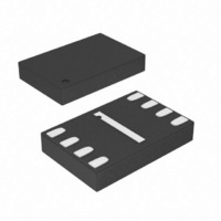
M24128-BFMB6TG STMicroelectronics, M24128-BFMB6TG Datasheet - Page 23

M24128-BFMB6TG
Manufacturer Part Number
M24128-BFMB6TG
Description
IC EEPROM 128KBIT 400KHZ 8MLP
Manufacturer
STMicroelectronics
Datasheet
1.M24128-BRMN6TP.pdf
(39 pages)
Specifications of M24128-BFMB6TG
Format - Memory
EEPROMs - Serial
Memory Type
EEPROM
Memory Size
128K (16K x 8)
Speed
400kHz
Interface
I²C, 2-Wire Serial
Voltage - Supply
1.7 V ~ 5.5 V
Operating Temperature
-40°C ~ 85°C
Package / Case
8-MLP, 8-UFDFPN
Ic Interface Type
I2C
Clock Frequency
400kHz
Access Time
900ns
Supply Voltage Range
1.7V To 5.5V
Memory Case Style
DFN
No. Of Pins
8
Operating Temperature Range
-40°C To +85°C
Rohs Compliant
Yes
Lead Free Status / RoHS Status
Lead free / RoHS Compliant
Available stocks
Company
Part Number
Manufacturer
Quantity
Price
Company:
Part Number:
M24128-BFMB6TG
Manufacturer:
RENESAS
Quantity:
3 122
Part Number:
M24128-BFMB6TG
Manufacturer:
ST
Quantity:
20 000
M24128-BW, M24128-BR, M24128-BF
Figure 12. AC test measurement I/O waveform
Table 11.
1. Characterized only.
Table 12.
1. Characterized value, not tested in production.
2. The device is not selected after power-up, after a Read command (after the Stop condition) or after the
Symbol
Z
Symbol
Z
t
WCH
WCL
completion of the internal write cycle t
NS
I
I
V
C
C
V
I
I
CC0
CC1
V
I
CC
LO
OL
LI
IN
IN
IH
IL
(1)
(1)
(1)
Input capacitance (SDA)
Input capacitance (other pins)
WC input impedance
WC input impedance
Pulse width ignored
(Input filter on SCL and SDA)
Input leakage current
(SCL, SDA, E2, E1, E0)
Output leakage current
Supply current (Read)
Supply current (Write)
Standby supply current
Standby supply current
Input low voltage (SDA,
SCL, WC)
Input high voltage
(SCL, SDA)
Input high voltage
(WC, E0, E1, E2)
Output low voltage
Input parameters
DC characteristics (M24xxx-W, device grade 6)
Parameter
Parameter
0.8V CC
0.2V CC
Input Levels
Doc ID 16892 Rev 19
W
(t
Device not selected
W
(in addition to those in
2.5 V < V
Device not selected
During t
is triggered by the correct decoding of a Write command).
SDA in Hi-Z, external voltage
I
applied on SDA: V
OL
device in Standby mode
I
OL
= 2.1 mA, V
or V
or V
V
= 3 mA, V
Test condition
Test condition
CC
W
V
V
IN
CC
CC
, 2.5 V < V
IN
IN
= V
< 5.5 V, f
, V
, V
< 0.3V
> 0.7V
Timing Reference Levels
SS
CC
CC
CC
CC
or V
= 5.5 V
= 2.5 V
(2)
(2)
CC
CC
SS
= 2.5 V or
Input and Output
c
CC
= 5.5 V
, V
, V
CC
= 400 kHz
or V
< 5.5 V
IN
Table
IN
= V
= V
AI00825B
CC
0.7V CC
0.3V CC
Min.
SS
SS
500
7)
50
DC and AC parameters
0.7V
0.7V
–0.45
Min.
CC
CC
Max.
200
100
8
6
V
0.3V
CC
Max.
5
± 2
± 2
6.5
0.4
2
5
2
(1)
+0.6
CC
Unit
pF
pF
k
k
ns
Unit
mA
mA
23/39
µA
µA
µA
µA
V
V
V
V


