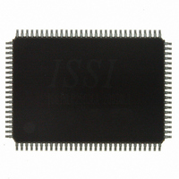
IS61NLP25636A-200TQLI ISSI, Integrated Silicon Solution Inc, IS61NLP25636A-200TQLI Datasheet - Page 24

IS61NLP25636A-200TQLI
Manufacturer Part Number
IS61NLP25636A-200TQLI
Description
IC SRAM 9MBIT 200MHZ 100TQFP
Manufacturer
ISSI, Integrated Silicon Solution Inc
Datasheet
1.IS61NLP25636A-200TQLI-TR.pdf
(37 pages)
Specifications of IS61NLP25636A-200TQLI
Format - Memory
RAM
Memory Type
SRAM - Synchronous
Memory Size
9M (256K x 36)
Speed
200MHz
Interface
Parallel
Voltage - Supply
3.135 V ~ 3.465 V
Operating Temperature
-40°C ~ 85°C
Package / Case
100-TQFP, 100-VQFP
Density
9Mb
Access Time (max)
3.1ns
Sync/async
Synchronous
Architecture
SDR
Clock Freq (max)
200MHz
Operating Supply Voltage (typ)
3.3V
Address Bus
18b
Package Type
TQFP
Operating Temp Range
-40C to 85C
Number Of Ports
4
Supply Current
280mA
Operating Supply Voltage (min)
3.135V
Operating Supply Voltage (max)
3.465V
Operating Temperature Classification
Industrial
Mounting
Surface Mount
Pin Count
100
Word Size
36b
Number Of Words
256K
Lead Free Status / RoHS Status
Lead free / RoHS Compliant
Other names
706-1102
IS61NLP25636A-200TQLI
IS61NLP25636A-200TQLI
Available stocks
Company
Part Number
Manufacturer
Quantity
Price
Company:
Part Number:
IS61NLP25636A-200TQLI
Manufacturer:
ISSI, Integrated Silicon Solution Inc
Quantity:
10 000
Part Number:
IS61NLP25636A-200TQLI
Manufacturer:
ISSI
Quantity:
20 000
Company:
Part Number:
IS61NLP25636A-200TQLI-TR
Manufacturer:
ISSI, Integrated Silicon Solution Inc
Quantity:
10 000
IS61NLP25636A/IS61NVP25636A
IS61NLP51218A/IS61NVP51218A
TEST DATA OUT (TDO)
The TDO output pin is used to serially clock data-out from
the registers.The output is active depending on the current
state of the TAP state machine (see TAP Controller State
Diagram). The output changes on the falling edge of TCK
and TDO is connected to the Least Significant Bit (LSB)
of any register.
PERFORMING A TAP RESET
A Reset is performed by forcing TMS HIGH (V
rising edges of TCK. RESET may be performed while the
SRAM is operating and does not affect its operation. At
power-up, the TAP is internally reset to ensure that TDO
comes up in a high-Z state.
TAP REGISTERS
Registers are connected between the TDI and TDO pins
and allow data to be scanned into and out of the SRAM
test circuitry. Only one register can be selected at a time
through the instruction registers. Data is serially loaded
into the TDI pin on the rising edge of TCK and output on
the TDO pin on the falling edge of TCK.
Instruction Register
Three-bit instructions can be serially loaded into the in-
struction register. This register is loaded when it is placed
between the TDI and TDO pins. (See TAP Controller Block
Diagram) At power-up, the instruction register is loaded
with the IDCODE instruction. It is also loaded with the
IDCODE instruction if the controller is placed in a reset
state as previously described.
When the TAP controller is in the CaptureIR state, the two
least significant bits are loaded with a binary “01” pattern to
allow for fault isolation of the board level serial test path.
Bypass Register
To save time when serially shifting data through registers,
it is sometimes advantageous to skip certain states. The
bypass register is a single-bit register that can be placed
between TDI and TDO pins. This allows data to be shifted
through the SRAM with minimal delay. The bypass reg-
ister is set LOW (V
executed.
IDENTIFICATION REGISTER DEFINITIONS
24
Instruction Field
Revision Number (31:28) Reserved for version number.
Device Depth (27:23)
Device Width (22:18)
ISSI Device ID (17:12)
ISSI JEDEC ID (11:1)
ID Register Presence (0) Indicate the presence of an ID register.
SS
) when the BYPASS instruction is
Description
Defines depth of SRAM. 256K or 512K
Defines width of the SRAM. x36 or x18
Reserved for future use.
Allows unique identification of SRAM vendor.
dd
Integrated Silicon Solution, Inc. — www.issi.com —
) for five
Boundary Scan Register
The boundary scan register is connected to all input and
output pins on the SRAM. Several no connect (NC) pins are
also included in the scan register to reserve pins for higher
density devices. The x36 configuration has a 75-bit-long
register and the x18 configuration also has a 75-bit-long
register. The boundary scan register is loaded with the
contents of the RAM Input and Output ring when the TAP
controller is in the Capture-DR state and then placed be-
tween the TDI and TDO pins when the controller is moved
to the Shift-DR state. The EXTEST, SAMPLE/PRELOAD
and SAMPLE-Z instructions can be used to capture the
contents of the Input and Output ring.
The Boundary Scan Order tables show the order in which
the bits are connected. Each bit corresponds to one of the
bumps on the SRAM package. The MSB of the register is
connected to TDI, and the LSB is connected to TDO.
Scan Register Sizes
Identification (ID) Register
The ID register is loaded with a vendor-specific, 32-bit
code during the Capture-DR state when the IDCODE com-
mand is loaded to the instruction register. The IDCODE
is hardwired into the SRAM and can be shifted out when
the TAP controller is in the Shift-DR state. The ID register
has vendor code and other information described in the
Identification Register Definitions table.
Register
Name
Instruction
Bypass
ID
Boundary Scan
Bit Size
00011010101 00011010101
(x18)
256K x 36
32
75
3
1
00111
00100
xxxxx
xxxx
1
Bit Size
(x36)
1-800-379-4774
32
75
3
1
512K x 18
01000
00011
xxxxx
xxxx
1
07/28/2010
Rev. G


