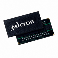
MT46H16M16LFBF-6:A TR Micron Technology Inc, MT46H16M16LFBF-6:A TR Datasheet - Page 27

MT46H16M16LFBF-6:A TR
Manufacturer Part Number
MT46H16M16LFBF-6:A TR
Description
IC DDR SDRAM 256MBIT 60VFBGA
Manufacturer
Micron Technology Inc
Type
DDR SDRAMr
Specifications of MT46H16M16LFBF-6:A TR
Format - Memory
RAM
Memory Type
Mobile DDR SDRAM
Memory Size
256M (16Mx16)
Speed
166MHz
Interface
Parallel
Voltage - Supply
1.7 V ~ 1.95 V
Operating Temperature
0°C ~ 70°C
Package / Case
60-VFBGA
Organization
16Mx16
Density
256Mb
Address Bus
15b
Access Time (max)
6.5/5ns
Maximum Clock Rate
166MHz
Operating Supply Voltage (typ)
1.8V
Package Type
VFBGA
Operating Temp Range
0C to 70C
Operating Supply Voltage (max)
1.95V
Operating Supply Voltage (min)
1.7V
Supply Current
100mA
Pin Count
60
Mounting
Surface Mount
Operating Temperature Classification
Commercial
Lead Free Status / RoHS Status
Lead free / RoHS Compliant
Other names
557-1319-2
Figure 12:
READs
PDF: 09005aef82091978 / Source: 09005aef8209195b
MT46H16M16LF__2.fm - Rev. H 6/08 EN
Command
BA0, BA1
A0–A12
CK#
CK
Example: Meeting
Bank x
Row
ACT
T0
READ burst operations are initiated with a READ command, as shown in Figure 13 on
page 28.
The starting column and bank addresses are provided with the READ command, and
auto precharge is either enabled or disabled for that burst access. If auto precharge is
enabled, the row being accessed is precharged at the completion of the burst. For the
READ commands used in the following illustrations, auto precharge is disabled.
During READ bursts, the valid data-out element from the starting column address will
be available following the CAS latency after the READ command. Each subsequent data-
out element will be valid nominally at the next positive or negative clock edge (for
example, at the next crossing of CK and CK#). Figure 14 on page 29 shows general timing
for different CAS latency settings. DQS is driven by the Mobile DDR SDRAM along with
output data. The initial LOW state on DQS is known as the read preamble; the LOW state
coincident with the last data-out element is known as the read postamble.
Upon completion of a burst, assuming no other commands have been initiated, the DQ
will go High-Z. A detailed explanation of
window hold), and the valid data window is depicted in Figure 37 on page 66. A detailed
explanation of
CK) is depicted in Figure 39 on page 68.
Data from any READ burst may be concatenated with or truncated with data from a
subsequent READ command. In either case, a continuous flow of data can be main-
tained. The first data element from the new burst either follows the last element of a
completed burst or the last desired data element of a longer burst that is being trun-
cated. The new READ command should be issued x cycles after the first READ
command, where x equals the number of desired data element pairs (pairs are required
by the 2n-prefetch architecture). This is shown in Figure 15 on page 30. A READ
command can be initiated on any clock cycle following a previous READ command.
Nonconsecutive read data is illustrated in Figure 16 on page 31. Full-speed random read
accesses within a page (or pages) can be performed, as shown in Figure 17 on page 32.
NOP
T1
t RRD
t
RCD (
NOP
t
DQSCK (DQS transition skew to CK) and
t
T2
RRD) MIN When 2 <
Bank y
Row
ACT
27
T3
Micron Technology, Inc., reserves the right to change products or specifications without notice.
t
256Mb: x16, x32 Mobile DDR SDRAM
RCD (
t
NOP
DQSQ (valid data-out skew),
T4
t
RRD) MIN
t RCD
NOP
T5
t
AC (data-out transition skew to
©2005 Micron Technology, Inc. All rights reserved.
RD/WR
Bank y
T6
Col
t
QH (data-out
Operations
Don’t Care
NOP
T7


