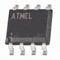
AT25128B-SSHL-B Atmel, AT25128B-SSHL-B Datasheet - Page 8

AT25128B-SSHL-B
Manufacturer Part Number
AT25128B-SSHL-B
Description
IC EEPROM 128KBIT 20MHZ 8SOIC
Manufacturer
Atmel
Datasheet
1.AT25128B-SSHL-B.pdf
(24 pages)
Specifications of AT25128B-SSHL-B
Format - Memory
EEPROMs - Serial
Memory Type
EEPROM
Memory Size
128K (16K x 8)
Speed
5MHz, 10MHz, 20MHz
Interface
SPI, 3-Wire Serial
Voltage - Supply
1.8 V ~ 5.5 V
Operating Temperature
-40°C ~ 85°C
Package / Case
8-SOIC (3.9mm Width)
Density
128Kb
Interface Type
Serial (SPI)
Organization
16Kx8
Access Time (max)
80ns
Frequency (max)
5MHz
Write Protection
Yes
Data Retention
100Year
Operating Supply Voltage (typ)
2.5/3.3/5V
Operating Temp Range
-40C to 85C
Supply Current
10mA
Operating Supply Voltage (min)
1.8V
Operating Supply Voltage (max)
5.5V
Operating Temperature Classification
Industrial
Mounting
Surface Mount
Pin Count
8
Memory Configuration
16384 X 8
Clock Frequency
3MHz
Supply Voltage Range
1.8V To 5.5V
Memory Case Style
SOIC
No. Of Pins
8
Rohs Compliant
Yes
Lead Free Status / RoHS Status
Lead free / RoHS Compliant
Available stocks
Company
Part Number
Manufacturer
Quantity
Price
Company:
Part Number:
AT25128B-SSHL-B
Manufacturer:
ATMEL
Quantity:
12 000
8
WRITE STATUS REGISTER (WRSR):
The AT25128B/256B is divided into four array segments. Top quarter (1/4), top half (1/2), or all of the memory seg-
ments can be protected. Any of the data within any selected segment will therefore be read only. The block write
protection levels and corresponding status register control bits are shown in
The three bits, BP0, BP1, and WPEN are nonvolatile cells that have the same properties and functions as the reg-
ular memory cells (e.g. WREN, tWC, RDSR)
Table 3-4.
The WRSR instruction also allows the user to enable or disable the write protect (WP) pin through the use of the
write protect enable (WPEN) bit. Hardware write protection is enabled when the WP pin is low and the WPEN bit is
“1”. Hardware write protection is disabled when either the WP pin is high or the WPEN bit is “0”. When the device is
hardware write protected, writes to the Status Register, including the Block Protect bits and the WPEN bit, and the
blockprotected sections in the memory array are disabled. Writes are only allowed to sections of the memory which
are not block-protected.
Note:
Table 3-5.
READ SEQUENCE (READ): Reading the AT25128B/256B via the SO pin requires the following sequence. After
the CS line is pulled low to select a device, the Read op-code is transmitted via the SI line followed by the byte
address to be read
specified address is then shifted out onto the SO line. If only one byte is to be read, the CS line should be driven
high after the data comes out. The read sequence can be continued since the byte address is automatically incre-
mented and data will continue to be shifted out. When the highest address is reached, the address counter will roll
over to the lowest address allowing the entire memory to be read in one continuous read cycle.
0
1 (1/4)
2 (1/2)
3 (All)
AT25128B/256B
WPEN
X
X
0
0
1
1
Level
When the WPEN bit is hardware write protected, it cannot be changed back to “0”, as long as the WP pin is held low.
Block Write Protect Bits.
WPEN Operation
High
High
Low
Low
WP
X
X
(Table
BP1
2-6). Upon completion, any data on the SI line will be ignored. The data (D7 - D0) at the
0
0
1
1
Status Register Bits
WEN
0
1
0
1
0
1
The WRSR instruction allows the user to select one of four levels of protection.
Protected Blocks
Protected
Protected
Protected
Protected
Protected
Protected
BP0
0
1
0
1
3000 – 3FFF
2000 – 3FFF
0000 – 3FFF
AT25128B
Unprotected
Array Addresses Protected
Protected
Protected
Protected
None
Writable
Writable
Writable
Blocks
Table
4000 – 7FFF
6000 – 7FFF
0000 – 7FFF
AT25256B
Status Register
None
Protected
Protected
Protected
Protected
Writable
Writable
2-4.
8698B–SEEPR–3/10


