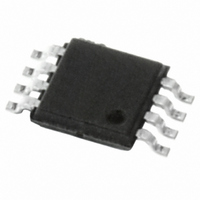
M95320-WDW6TP STMicroelectronics, M95320-WDW6TP Datasheet - Page 19

M95320-WDW6TP
Manufacturer Part Number
M95320-WDW6TP
Description
IC EEPROM 32KBIT 10MHZ 8TSSOP
Manufacturer
STMicroelectronics
Datasheet
1.M95320-WMN6TP.pdf
(44 pages)
Specifications of M95320-WDW6TP
Format - Memory
EEPROMs - Serial
Memory Type
EEPROM
Memory Size
32K (4K x 8)
Speed
10MHz
Interface
SPI, 3-Wire Serial
Voltage - Supply
2.5 V ~ 5.5 V
Operating Temperature
-40°C ~ 85°C
Package / Case
8-TSSOP
Lead Free Status / RoHS Status
Lead free / RoHS Compliant
Other names
497-8693-2
M95320-WDW6TP
M95320-WDW6TP
Available stocks
Company
Part Number
Manufacturer
Quantity
Price
Company:
Part Number:
M95320-WDW6TP
Manufacturer:
STMicroelectronics
Quantity:
135
Company:
Part Number:
M95320-WDW6TP
Manufacturer:
ST
Quantity:
4 066
Part Number:
M95320-WDW6TP
Manufacturer:
ST
Quantity:
20 000
M95320, M95320-W, M95320-R
6.4
Figure 9.
Write Status Register (WRSR)
The Write Status Register (WRSR) instruction allows new values to be written to the Status
Register. Before it can be accepted, a Write Enable (WREN) instruction must previously
have been executed.
The Write Status Register (WRSR) instruction is entered by driving Chip Select (S) low,
sending the instruction code followed by the data byte on Serial Data input (D), and driving
the Chip Select (S) signal high. Chip Select (S) must be driven high after the rising edge of
Serial Clock (C) that latches in the eighth bit of the data byte, and before the next rising edge
of Serial Clock (C). Otherwise, the Write Status Register (WRSR) instruction is not
executed.
Driving the Chip Select (S) signal high at a byte boundary of the input data triggers the self-
timed write cycle that takes t
Table
While the Write Status Register cycle is in progress, the Status Register may still be read to
check the value of the Write in progress (WIP) bit: the WIP bit is 1 during the self-timed write
cycle t
reset at the end of the write cycle t
The Write Status Register (WRSR) instruction allows the user to change the values of the
BP1, BP0 bits and the SRWD bit:
●
●
The contents of the SRWD and BP1, BP0 bits are updated after the completion of the
WRSR instruction, including the t
The Write Status Register (WRSR) instruction has no effect on the b6, b5, b4, b1 and b0
bits in the Status Register. Bits b6, b5, b4 are always read as 0.
The Block protect (BP1, BP0) bits define the size of the area that is to be treated as
read only, as defined in
The SRWD bit (Status register write disable bit), in accordance with the signal read on
the Write protect pin (W), allows the user to set or reset the write protection mode of the
Status Register itself, as shown in
Write Status Register (WRSR) instruction is not executed.
20). The instruction sequence is shown in
W
, and is 0 when the write cycle is complete. The WEL bit (Write enable latch) is also
S
C
D
Q
Read Status Register (RDSR) sequence
0
High Impedance
1
2
Instruction
3 4 5 6 7 8 9 10 11 12 13 14 15
W
Table
Doc ID 5711 Rev 12
to complete (as specified in
W
W
2.
write cycle.
.
MSB
7 6 5 4 3 2 1 0
Table
Status Register Out
5. When in the Write-protected mode, the
Figure
10.
MSB
7 6 5 4 3 2 1 0
Table
Status Register Out
17,
Table
18,
7
AI02031E
Table
Instructions
19,
19/44


