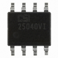
CAT25040VI-GT3 ON Semiconductor, CAT25040VI-GT3 Datasheet - Page 5

CAT25040VI-GT3
Manufacturer Part Number
CAT25040VI-GT3
Description
IC EEPROM 4KBIT 10MHZ 8SOIC
Manufacturer
ON Semiconductor
Datasheet
1.CAT25020VI-GT3.pdf
(15 pages)
Specifications of CAT25040VI-GT3
Format - Memory
EEPROMs - Serial
Memory Type
EEPROM
Memory Size
4K (512 x 8)
Speed
10MHz
Interface
SPI, 3-Wire Serial
Voltage - Supply
1.8 V ~ 5.5 V
Operating Temperature
-40°C ~ 85°C
Package / Case
8-SOIC (3.9mm Width)
Lead Free Status / RoHS Status
Lead free / RoHS Compliant
Other names
25040VI-GT3
CAT25040VI-GT3TR
CAT25040VI-GT3TR
Available stocks
Company
Part Number
Manufacturer
Quantity
Price
Company:
Part Number:
CAT25040VI-GT3
Manufacturer:
PHILIPS
Quantity:
456
Part Number:
CAT25040VI-GT3
Manufacturer:
ON/安森美
Quantity:
20 000
Company:
Part Number:
CAT25040VI-GT3JN
Manufacturer:
ON Semiconductor
Quantity:
2 250
disable state. The device contains a Write Enable Latch
(WEL) which must be set before attempting to write to the
memory array or to the status register. In addition, the
address of the memory location(s) to be written must be
outside the protected area, as defined by BP0 and BP1 bits
from the status register.
Write Enable and Write Disable
Status Register WEL bit are set by sending the WREN
Table 8. STATUS REGISTER
Table 9. BLOCK PROTECTION BITS
The CAT25010/20/40 device powers up into a write
The internal Write Enable Latch and the corresponding
BP1
7
1
SCK
Status Register Bits
0
0
1
1
SO
CS
SI
SCK
SO
CS
SI
Dashed Line = mode (1, 1)
Dashed Line = mode (1, 1)
6
1
BP0
0
1
0
1
None
CAT25010: 060−07F, CAT25020: 0C0−0FF, CAT25040: 180−1FF
CAT25010: 040−07F, CAT25020: 080−0FF, CAT25040: 100−1FF
CAT25010: 000−07F, CAT25020: 000−0FF, CAT25040: 000−1FF
5
1
0
0
Figure 3. WREN Timing
WRITE OPERATIONS
0
0
Figure 4. WRDI Timing
http://onsemi.com
4
1
Array Address Protected
0
0
HIGH IMPEDANCE
0
0
HIGH IMPEDANCE
5
0
0
instruction to the CAT25010/20/40. Care must be taken to
take the CS input high after the WREN instruction, as
otherwise the Write Enable Latch will not be properly set.
WREN timing is illustrated in Figure 3. The WREN
instruction must be sent prior to any WRITE or WRSR
instruction.
WRDI instruction as shown in Figure 4. Disabling write
operations by resetting the WEL bit, will protect the device
against inadvertent writes.
1
The internal write enable latch is reset by sending the
BP1
1
3
1
0
0
0
BP0
2
No Protection
Quarter Array Protection
Half Array Protection
Full Array Protection
WEL
1
Protection
RDY
0


