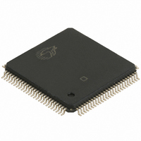
CY7C028-15AC Cypress Semiconductor Corp, CY7C028-15AC Datasheet

CY7C028-15AC
Specifications of CY7C028-15AC
Available stocks
Related parts for CY7C028-15AC
CY7C028-15AC Summary of contents
Page 1
... Features • True Dual-Ported memory cells which allow simulta- neous access of the same memory location • 32K x 16 organization (CY7C027) • 64K x 16 organization (CY7C028) • 32K x 18 organization (CY7C037) • 64K x 18 organization (CY7C038) • 0.35-micron CMOS for optimum speed/power [1] • ...
Page 2
... An automatic power-down feature is controlled independently on each port by the chip enable pins. The CY7C027/028 and CY7C037/038 are available in 100-pin Thin Quad Plastic Flatpack (TQFP) packages. 100-Pin TQFP (Top View CY7C028 (64K x 16) CY7C027 (32K x 16 CY7C027/028 CY7C037/038 ), read or write enable (R/W), and output enable ...
Page 3
Pin Configurations (continued) 100 99 98 A9L 1 A10L 2 A11L 3 A12L 4 A13L 5 A14L 6 [7] A15L 7 LBL 8 UBL 9 CE0L 10 CE1L 11 SEML 12 R/WL 13 OEL 14 VCC 15 GND 16 I/O17L ...
Page 4
... High Z State ............................................ –0.5V to +7.0DC Note: 8. The Voltage on any input or I/O pin cannot exceed the power pin during power-up. 9. Pulse width < 20 ns. 10. Industrial parts are available in CY7C028 and CY7C038 only. Document #: 38-06042 Rev. *A Chip Enable (CE is LOW when CE 1R Read/Write Enable Output Enable Address (A – ...
Page 5
Electrical Characteristics Over the Operating Range Symbol Parameter V Output HIGH Voltage ( –4.0 mA Output LOW Voltage ( +4.0 mA Input HIGH Voltage IH V Input LOW Voltage ...
Page 6
Capacitance Parameter Description C Input Capacitance IN C Output Capacitance OUT AC Test Loads and Waveforms 893 OUTPUT 347 (a) Normal Load (Load 1) AC Test Loads (Applicable to -12 ...
Page 7
Switching Characteristics Over the Operating Range Parameter Description READ CYCLE t Read Cycle Time RC t Address to Data Valid AA t Output Hold From Address Change OHA [15 LOW to Data Valid ACE t OE LOW to ...
Page 8
Switching Characteristics Over the Operating Range Parameter Description [20] BUSY TIMING t BUSY LOW from Address Match BLA t BUSY HIGH from Address Mismatch BHA t BUSY LOW from CE LOW BLC t BUSY HIGH from CE HIGH BHC t ...
Page 9
Switching Waveforms Read Cycle No. 1 (Either Port Address Access) ADDRESS t OHA DATA OUT PREVIOUS DATA VALID Read Cycle No. 2 (Either Port CE/OE Access) CE and DATA OUT I CC CURRENT I SB [23, ...
Page 10
Switching Waveforms (continued) Write Cycle No. 1: R/W Controlled Timing ADDRESS OE [32,33 R/W NOTE 35 DATA OUT DATA IN Write Cycle No Controlled Timing ADDRESS [32,33 R/W DATA IN Notes: 28. ...
Page 11
Switching Waveforms (continued) Semaphore Read After Write Timing, Either Side A –A VALID ADRESS 0 2 SEM I R/W OE Timing Diagram of Semaphore Contention A – R/W L SEM L A – ...
Page 12
Switching Waveforms (continued) Timing Diagram of Read with BUSY (M/S=HIGH) ADDRESS R R/W R DATA ADDRESS L BUSY L DATA OUTL Write Timing with Busy Input (M/S=LOW) R/W BUSY Note: 41 LOW. ...
Page 13
Switching Waveforms (continued) Busy Timing Diagram No.1 (CE Arbitration) CE Valid First: L ADDRESS L BUSY R CE ValidFirst: R ADDRESS L BUSY L Busy Timing Diagram No. 2 (Address Arbitration) Left ...
Page 14
... Switching Waveforms (continued) Interrupt Timing Diagrams Left Side Sets INT : R ADDRESS WRITE 7FFF (FFFF for CY7C028/38 R/W L INT R [44] t INS Right Side Clears INT : R ADDRESS R INT R : Right Side Sets INT L ADDRESS WRITE 7FFE (FFFE for CY7C028/38 R/W R INT L t INS Left Side Clears INT ...
Page 15
... CY7C027/37, FFFF for the CY7C028/38) is the mailbox for the right port and the second-highest memory location (7FFE for the CY7C027/37, FFFE for the CY7C028/38) is the mailbox for the left port. When one port writes to the other port’s mailbox, an interrupt is generated to the owner. The interrupt is reset when the owner reads the contents of the mailbox ...
Page 16
... Left port writes 1 to semaphore Right port writes 0 to semaphore Right port writes 1 to semaphore Left port writes 0 to semaphore Left port writes 1 to semaphore Notes: 45. A and A , FFFF/FFFE for the CY7C028/038. 0L–15L 0R–15R 46. If BUSY =L, then no change. R 47. If BUSY =L, then no change. ...
Page 17
... Asynchronous Dual-Port SRAM Speed (ns) Ordering Code [1] 12 CY7C027-12AC 15 CY7C027-15AC 20 CY7C027-20AC 64K x16 Asynchronous Dual-Port SRAM Speed (ns) Ordering Code [1] 12 CY7C028-12AC 15 CY7C028-15AC 20 CY7C028-20AC CY7C028-20AI 32K x18 Asynchronous Dual-Port SRAM Speed (ns) Ordering Code [1] 12 CY7C037-12AC 15 CY7C037-15AC 20 CY7C037-20AC 64K x18 Asynchronous Dual-Port SRAM Speed (ns) Ordering Code ...
Page 18
... Document #: 38-06042 Rev. *A © Cypress Semiconductor Corporation, 2001. The information contained herein is subject to change without notice. Cypress Semiconductor Corporation assumes no responsibility for the use of any circuitry other than circuitry embodied in a Cypress Semiconductor product. Nor does it convey or imply any license under patent or other rights. Cypress Semiconductor does not authorize its products for use as critical components in life-support systems where a malfunction or failure may reasonably be expected to result in significant injury to the user ...
Page 19
Document Title: CY7C027/028, CY7C037/038 32K/64K x 16/18 Dual-Port Static RAM Document Number: 38-06042 Issue REV. ECN NO. Date ** 110190 09/29/01 *A 122292 12/27/02 Document #: 38-06042 Rev. *A Orig. of Change Description of Change SZV Change from Spec number: ...


