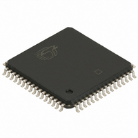
CY7C144AV-25AXC Cypress Semiconductor Corp, CY7C144AV-25AXC Datasheet

CY7C144AV-25AXC
Specifications of CY7C144AV-25AXC
CY7C144AV-25AXC
Available stocks
Related parts for CY7C144AV-25AXC
CY7C144AV-25AXC Summary of contents
Page 1
... CY7C138AV CY7C139AV CY7C144AV CY7C145AV CY7C006AV CY7C016AV CY7C007AV CY7C017AV 3.3V 4K/8K/16K/32K x 8/9 Dual-Port Static RAM Features • True Dual-Ported memory cells which allow simultaneous access of the same memory location • 4K/8K/16K/32K x 8 organizations (CY7C0138AV/144AV/006AV/007AV) • 4K/8K/16K/32K x 9 organizations (CY7C0139AV/145AV/016AV/017AV) • 0.35-micron CMOS for optimum speed/power • ...
Page 2
... CY7C139AV I/O on the CY7C145AV I/O on the CY7C145AV. 8R Document #: 38-06051 Rev. *C 68-Pin PLCC Top View CY7C138AV ( CY7C139AV ( 2728 29 30 3132 68-Pin PLCC Top View CY7C144AV ( CY7C145AV ( 2728 29 30 3132 CY7C138AV/144AV/006AV CY7C139AV/145AV/016AV CY7C007AV/017AV INT 54 L BUSY 53 L GND 52 51 M/S BUSY INT ...
Page 3
... I/O 3R I/O 4R I/O 5R I/O6 R Notes: 8. I/O for CY7C016AV and CY7C017AV only. NC for other parts. 9. Address line for CY7C007AV and CY7C017AV only. NC for other parts. Document #: 38-06051 Rev. *C 64-Pin TQFP Top View CY7C144AV ( 68-Pin PLCC Top View CY7C006AV (16K CY7C007AV (32K CY7C016AV (16K x 9) ...
Page 4
Pin Configurations (continued) I/O 2L I/O 3L I/O 4L I/O 5L GND I GND I/O 0R I I/O 3R I/O 4R I/O 5R Selection Guide Maximum Access Time (ns) Typical ...
Page 5
... Interrupts The upper two memory locations may be used for message passing. The highest memory location (FFF for the CY7C138AV/9AV, 1FFF for the CY7C144AV/5AV, 3FFF for the CY7C006AV/16AV, 7FFF for the CY7C007AV/17AV) is the mailbox for the right port and the second-highest memory ...
Page 6
... HIGH during SEM LOW). A after an semaphore address. OE and R/W are used in the same BLA manner as a normal memory access. When writing or reading a semaphore, the other address pins have no effect. When writing to the semaphore, only I/O written to the left port of an available semaphore, a one will appear at the same semaphore address on the right port ...
Page 7
Maximum Ratings (Above which the useful life may be impaired. For user guide- lines, not tested.) Storage Temperature .................................–65 Ambient Temperature with Power Applied.............................................–55 Supply Voltage to Ground Potential ............... –0.5V to +4.6V DC Voltage Applied to Outputs in ...
Page 8
AC Test Loads and Waveforms 3. 590Ω OUTPUT 435Ω (a) Normal Load (Load 1) 3.0V GND . Switching Characteristics Over the Operating Range Parameter Description READ CYCLE t Read Cycle Time RC ...
Page 9
Switching Characteristics Over the Operating Range Parameter Description t Data Hold From Write End HD [18, 19] t R/W LOW to High Z HZWE [18, 19] t R/W HIGH to Low Z LZWE [20] t Write Pulse to Data Delay ...
Page 10
Switching Waveforms Read Cycle No. 1 (Either Port Address Access) ADDRESS OHA DATA OUT PREVIOUS DATA VALID Read Cycle No. 2 (Either Port CE/OE Access DATA OUT CURRENT I SB [24, ...
Page 11
Switching Waveforms (continued) Write Cycle No. 1: R/W Controlled Timing ADDRESS OE [34 R/W Note 35 DATA OUT DATA IN Write Cycle No Controlled Timing ADDRESS [34 R/W DATA IN Notes: 29. ...
Page 12
Switching Waveforms (continued) Semaphore Read After Write Timing, Either Side A –A VALID ADRESS SEM I R/W OE Timing Diagram of Semaphore Contention A – R/W L SEM L A –A ...
Page 13
Switching Waveforms (continued) Timing Diagram of Read with BUSY (M/S=HIGH) ADDRESS R R/W R DATA ADDRESS L BUSY L DATA OUTL Write Timing with Busy Input (M/S=LOW) R/W BUSY Note: 41 LOW. ...
Page 14
Switching Waveforms (continued) Busy Timing Diagram No. 1 (CE Arbitration) CE Valid First: L ADDRESS L BUSY R CE Valid First: R ADDRESS L BUSY L Busy Timing Diagram No. 2 (Address ...
Page 15
Switching Waveforms (continued) Interrupt Timing Diagrams Left Side Sets INT : R ADDRESS WRITE FFF (See Functional Description R/W L INT R [44] t INS Right Side Clears INT : R ADDRESS R/W R ...
Page 16
Table 1. Non-Contending Read/Write Inputs CE R/W OE SEM High Data Out High Data Data Out L L ...
Page 17
... CY7C139AV–20JC 25 CY7C139AV–25JC 8K x8 3.3V Asynchronous Dual-Port SRAM Speed (ns) Ordering Code 20 CY7C144AV–20AC CY7C144AV–20JC 25 CY7C144AV–25AC CY7C144AV-25AXC CY7C144AV–25JC CY7C144AV-25JXC 8K x9 3.3V Asynchronous Dual-Port SRAM Speed (ns) Ordering Code 20 CY7C145AV–20JC 25 CY7C145AV–25JC 16K x8 3.3V Asynchronous Dual-Port SRAM Speed (ns) ...
Page 18
Ordering Information (continued) 16K x9 3.3V Asynchronous Dual-Port SRAM Speed (ns) Ordering Code 20 CY7C016AV–20JC 25 CY7C016AV–25JC 32K x8 3.3V Asynchronous Dual-Port SRAM Speed (ns) Ordering Code 20 CY7C007AV–20JC CY7C007AV–20JI 25 CY7C007AV–25JC 32K x9 3.3V Asynchronous Dual-Port SRAM Speed (ns) ...
Page 19
... Document #: 38-06051 Rev. *C © Cypress Semiconductor Corporation, 2005. The information contained herein is subject to change without notice. Cypress Semiconductor Corporation assumes no responsibility for the use of any circuitry other than circuitry embodied in a Cypress product. Nor does it convey or imply any license under patent or other rights. Cypress products are not warranted nor intended to be used for medical, life support, life saving, critical control or safety applications, unless pursuant to an express written agreement with Cypress ...
Page 20
... PCX Document #: 38-06051 Rev. *C Description of Change Change from Spec number: 38-00837 to 38-06051 RBI Power up requirements added to Maximum Ratings Information Removed cross information from features section Added Pb-Free Logo Added Pb-Free parts to ordering information: CY7C144AV-25AXC, CY7C144AV-25JXC, CY7C006AV-25AXC CY7C138AV/144AV/006AV CY7C139AV/145AV/016AV CY7C007AV/017AV Page [+] Feedback ...


