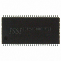
IS42S16400F-7TLI ISSI, Integrated Silicon Solution Inc, IS42S16400F-7TLI Datasheet - Page 10

IS42S16400F-7TLI
Manufacturer Part Number
IS42S16400F-7TLI
Description
IC SDRAM 64MBIT 143MHZ 54TSOP
Manufacturer
ISSI, Integrated Silicon Solution Inc
Type
SDRAMr
Specifications of IS42S16400F-7TLI
Format - Memory
RAM
Memory Type
SDRAM
Memory Size
64M (4M x 16)
Speed
143MHz
Interface
Parallel
Voltage - Supply
3 V ~ 3.6 V
Operating Temperature
-40°C ~ 85°C
Package / Case
54-TSOP II
Organization
4Mx16
Density
64Mb
Address Bus
14b
Access Time (max)
6/5.4ns
Maximum Clock Rate
143MHz
Operating Supply Voltage (typ)
3.3V
Package Type
TSOP-II
Operating Temp Range
-40C to 85C
Operating Supply Voltage (max)
3.6V
Operating Supply Voltage (min)
3V
Supply Current
110mA
Pin Count
54
Mounting
Surface Mount
Operating Temperature Classification
Industrial
Data Bus Width
16 bit
Maximum Clock Frequency
143 MHz
Access Time
6 ns, 5.4 ns
Supply Voltage (max)
3.6 V
Supply Voltage (min)
3 V
Maximum Operating Current
110 mA
Maximum Operating Temperature
+ 85 C
Minimum Operating Temperature
- 40 C
Mounting Style
SMD/SMT
Lead Free Status / RoHS Status
Lead free / RoHS Compliant
Other names
706-1078
IS42S16400F-7TLI
IS42S16400F-7TLI
Available stocks
Company
Part Number
Manufacturer
Quantity
Price
Company:
Part Number:
IS42S16400F-7TLI
Manufacturer:
BEL
Quantity:
100
Company:
Part Number:
IS42S16400F-7TLI
Manufacturer:
ISSI
Quantity:
5 530
Company:
Part Number:
IS42S16400F-7TLI
Manufacturer:
ISSI
Quantity:
6 250
Company:
Part Number:
IS42S16400F-7TLI
Manufacturer:
ISSI
Quantity:
1 000
Part Number:
IS42S16400F-7TLI
Manufacturer:
ISSI
Quantity:
20 000
Company:
Part Number:
IS42S16400F-7TLI-TR**MG-Z
Manufacturer:
ISSI
Quantity:
1 648
IS42S16400F
IC42S16400F
10
10. For a READ without auto precharge interrupted by a READ (with or without auto precharge), the READ to bank m will interrupt
11. For a READ without auto precharge interrupted by a WRITE (with or without auto precharge), the WRITE to bank m will inter-
12. For a WRITE without auto precharge interrupted by a READ (with or without auto precharge), the READ to bank m will interrupt
13. For a WRITE without auto precharge interrupted by a WRITE (with or without auto precharge), the WRITE to bank m will inter-
14. For a READ with auto precharge interrupted by a READ (with or without auto precharge), the READ to bank m will interrupt the
15. For a READ with auto precharge interrupted by a WRITE (with or without auto precharge), the WRITE to bank m will interrupt
16. For a WRITE with auto precharge interrupted by a READ (with or without auto precharge), the READ to bank m will interrupt
17. For a WRITE with auto precharge interrupted by a WRITE (with or without auto precharge), the WRITE to bank m will interrupt
8. CONCURRENT AUTO PRECHARGE: Bank n will initiate the AUTO PRECHARGE command when its burst has been inter-
9. Burst in bank n continues as initiated.
rupted by bank m’s burst.
the READ on bank n, CAS latency later (Consecutive READ Bursts).
rupt the READ on bank n when registered (READ to WRITE). DQM should be used one clock prior to the WRITE command to
prevent bus contention.
the WRITE on bank n when registered (WRITE to READ), with the data-out appearing CAS latency later. The last valid WRITE
to bank n will be data-in registered one clock prior to the READ to bank m.
rupt the WRITE on bank n when registered (WRITE to WRITE). The last valid WRITE to bank n will be data-in registered one
clock prior to the READ to bank m.
READ on bank n, CAS latency later. The PRECHARGE to bank n will begin when the READ to bank m is registered (Fig CAP
1).
the READ on bank n when registered. DQM should be used two clocks prior to the WRITE command to prevent bus contention.
The PRECHARGE to bank n will begin when the WRITE to bank m is registered (Fig CAP 2).
the WRITE on bank n when registered, with the data-out appearing CAS latency later. The PRECHARGE to bank n will begin
after t
tered one clock prior to the READ to bank m (Fig CAP 3).
the WRITE on bank n when registered. The PRECHARGE to bank n will begin after t
WRITE to bank m is registered. The last valid WRITE to bank n will be data registered one clock prior to the WRITE to bank m
(Fig CAP 4).
WR
is met, where t
wr
begins when the READ to bank m is registered. The last valid WRITE to bank n will be data-in regis-
Integrated Silicon Solution, Inc. — www.issi.com
wr
is met, where t WR begins when the
03/19/08
Rev. A


