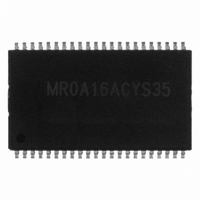
MR0A16ACYS35 EverSpin Technologies Inc, MR0A16ACYS35 Datasheet

MR0A16ACYS35
Specifications of MR0A16ACYS35
MR0A16ACYS35
Available stocks
Related parts for MR0A16ACYS35
MR0A16ACYS35 Summary of contents
Page 1
... MRAM is a nonvolatile memory technology that protects data in the event of power loss and does not require periodic refreshing. The MR0A16A is the ideal memory solution for applications that must permanently store and retrieve critical data quickly. The MR0A16A is available in a 400-mil, 44-lead ...
Page 2
... MR0A16A Advanced Information Data Sheet, Rev UPPER BYTE OUTPUT ENABLE LOWER BYTE OUTPUT ENABLE 8 8 ROW COLUMN DECODER DECODER SENSE AMPS 16 64K x 16 BIT MEMORY ARRAY 16 FINAL WRITE DRIVERS UPPER BYTE WRITE ENABLE LOWER BYTE WRITE ENABLE Figure 1. Block Diagram Table 1. Pin Functions Signal Name A[15: ...
Page 3
NOTES high ...
Page 4
... Parameter Power supply voltage Write inhibit voltage Input high voltage Input low voltage Operating temperature MR0A16AYS35 (Commercial) MR0A16ACYS35 (Industrial) MR0A16AVYS35 (Extended) NOTES: 1 After power must remain high for 2 ms. Memory is designed to prevent writing for all input pin conditions if V falls below minimum V ...
Page 5
Direct Current (dc) Parameter Input leakage current Output leakage current Output low voltage ( mA +100 μ Output high voltage (I = –4 mA –100 mA) OH Parameter ac active supply ...
Page 6
Electrical Specifications Logic input timing measurement reference level Logic output timing measurement reference level Logic input pulse levels Input rise/fall time Output load for low and high impedance parameters Output load for all other timing parameters OUTPUT MR0A16A Advanced Information ...
Page 7
Timing Specifications Read Mode Parameter Read cycle time Address access time 3 Enable access time Output enable access time Byte enable access time Output hold from address change Enable low to output active Output enable low to output active Byte ...
Page 8
Timing Specifications A (ADDRESS) Q (DATA OUT) PREVIOUS DATA VALID NOTES: 1 Device is continuously selected (E ≤ (ADDRESS) E (CHIP ENABLE) G (OUTPUT ENABLE) LB, UB (BYTE ENABLE) Q (DATA OUT) MR0A16A Advanced Information Data Sheet, Rev. ...
Page 9
Write Mode Table 10. Write Cycle Timing 1 (W Controlled) Parameter 6 Write cycle time Address set-up time Address valid to end of write (G high) Address valid to end of write (G low) Write pulse width (G high) Write ...
Page 10
Timing Specifications A (ADDRESS) E (CHIP ENABLE) W (WRITE ENABLE) LB, UB (BYTE ENABLE) D (DATA IN) Hi-Z Q (DATA OUT) MR0A16A Advanced Information Data Sheet, Rev AVAV t AVWH t WLEH t WLWH t AVWL t ...
Page 11
Table 11. Write Cycle Timing 2 (E Controlled) Parameter 6 Write cycle time Address set-up time Address valid to end of write (G high) Address valid to end of write (G low) Enable to end of write (G high) Enable ...
Page 12
Timing Specifications A (ADDRESS) E (CHIP ENABLE) W (WRITE ENABLE) LB, UB (BYTE ENABLE) D (DATA IN) Q (DATA OUT) MR0A16A Advanced Information Data Sheet, Rev AVAV t AVEH t AVEL Hi-Z Figure 7. Write Cycle 2 ...
Page 13
Table 12. Write Cycle Timing 3 (LB/UB Controlled) Parameter 7 Write cycle time Address set-up time Address valid to end of write (G high) Address valid to end of write (G low) Byte pulse width (G high) Byte pulse width ...
Page 14
Timing Specifications A (ADDRESS) E (CHIP ENABLE) LB, UB (BYTE ENABLE) W (WRITE ENABLE) D (DATA IN) Hi-Z Q (DATA OUT) Figure 8. Write Cycle 3 (LB/UB Controlled) MR0A16A Advanced Information Data Sheet, Rev AVAV t AVBH ...
Page 15
... Industrial, Extended — Typically 10 year applications - installed telecom equipment, workstations, servers, etc. These products can also be used in Commercial applications. Part Numbering System MR Freescale MRAM Memory Prefix Density Code ( Mb) Memory Type (A = async sync) Package Information Pin Package Device Count MR0A16A ...
Page 16
Mechanical Drawing Mechanical Drawing The following pages detail the package available to MR0A16A. MR0A16A Advanced Information Data Sheet, Rev Freescale Semiconductor ...
Page 17
...
Page 18
...
Page 19
...
Page 20
How to Reach Us: USA/Europe/Locations not listed: Freescale Semiconductor Literature Distribution P.O. Box 5405, Denver, Colorado 80217 1-800-521-6274 or 480-768-2130 Japan: Freescale Semiconductor Japan Ltd. SPS, Technical Information Center 3-20-1, Minami-Azabu Minato-ku Tokyo 106-8573, Japan 81-3-3440-3569 Asia/Pacific: Freescale Semiconductor H.K. ...


