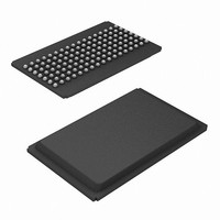
CY7C1370D-200BGXC Cypress Semiconductor Corp, CY7C1370D-200BGXC Datasheet - Page 11

CY7C1370D-200BGXC
Manufacturer Part Number
CY7C1370D-200BGXC
Description
IC SRAM 18MBIT 200MHZ 119BGA
Manufacturer
Cypress Semiconductor Corp
Type
Synchronousr
Specifications of CY7C1370D-200BGXC
Memory Size
18M (512K x 36)
Package / Case
119-BGA
Format - Memory
RAM
Memory Type
SRAM - Synchronous
Speed
200MHz
Interface
Parallel
Voltage - Supply
3.135 V ~ 3.6 V
Operating Temperature
0°C ~ 70°C
Access Time
3 ns
Maximum Clock Frequency
200 MHz
Supply Voltage (max)
3.6 V
Supply Voltage (min)
3.135 V
Maximum Operating Current
300 mA
Maximum Operating Temperature
+ 70 C
Minimum Operating Temperature
0 C
Mounting Style
SMD/SMT
Number Of Ports
4
Operating Supply Voltage
3.3 V
Lead Free Status / RoHS Status
Lead free / RoHS Compliant
Lead Free Status / RoHS Status
Lead free / RoHS Compliant, Lead free / RoHS Compliant
Available stocks
Company
Part Number
Manufacturer
Quantity
Price
Company:
Part Number:
CY7C1370D-200BGXC
Manufacturer:
Cypress Semiconductor Corp
Quantity:
10 000
IEEE 1149.1 Serial Boundary Scan (JTAG)
The CY7C1370DV25/CY7C1372DV25 incorporates a serial
boundary scan test access port (TAP).This part is fully compliant
with 1149.1. The TAP operates using JEDEC-standard 3.3 V or
2.5 V I/O logic levels.
The
controller, instruction register, boundary scan register, bypass
register, and ID register.
Disabling the JTAG Feature
It is possible to operate the SRAM without using the JTAG
feature. To disable the TAP controller, TCK must be tied LOW
(V
internally pulled up and may be unconnected. They may
alternately be connected to V
should be left unconnected. Upon power-up, the device will
come up in a reset state which will not interfere with the operation
of the device.
TAP Controller State Diagram
The 0/1 next to each state represents the value of TMS at the
rising edge of TCK.
Document Number: 38-05558 Rev. *H
Read
Write – no bytes written
Write byte a – (DQ
Write byte b – (DQ
Write both bytes
SS
1
0
) to prevent clocking of the device. TDI and TMS are
TEST-LOGIC
RUN-TEST/
CY7C1370DV25/CY7C1372DV25
RESET
IDLE
0
1
a
b
Function (CY7C1372DV25)
and DQP
and DQP
1
0
CAPTURE-DR
UPDATE-DR
PAUSE-DR
DR-SCAN
SHIFT-DR
EXIT1-DR
EXIT2-DR
1
SELECT
0
0
1
0
1
1
DD
0
a
b
)
)
through a pull-up resistor. TDO
1
1
0
0
contains
1
0
CAPTURE-IR
UPDATE-IR
PAUSE-IR
1
IR-SCAN
SHIFT-IR
EXIT1-IR
EXIT2-IR
SELECT
0
0
1
0
1
1
0
a
1
1
0
0
TAP
Test Access Port (TAP)
Test Clock (TCK)
The test clock is used only with the TAP controller. All inputs are
captured on the rising edge of TCK. All outputs are driven from
the falling edge of TCK.
Test Mode Select (TMS)
The TMS input is used to give commands to the TAP controller
and is sampled on the rising edge of TCK. It is allowable to leave
this ball unconnected if the TAP is not used. The ball is pulled up
internally, resulting in a logic HIGH level.
Test Data-In (TDI)
The TDI ball is used to serially input information into the registers
and can be connected to the input of any of the registers. The
register between TDI and TDO is chosen by the instruction that
is loaded into the TAP instruction register. For information on
loading the instruction register, see
Diagram. TDI is internally pulled up and can be unconnected if
the TAP is unused in an application. TDI is connected to the most
significant bit (MSB) of any register. (See
Diagram on page
Test Data-Out (TDO)
The TDO output ball is used to serially clock data-out from the
registers. The output is active depending upon the current state
of the TAP state machine. The output changes on the falling edge
of TCK. TDO is connected to the least significant bit (LSB) of any
register. (See
WE
H
L
L
L
L
TAP Controller State
12.)
BW
H
H
x
L
L
b
Diagram.)
CY7C1370DV25
CY7C1372DV25
TAP Controller State
TAP Controller Block
BW
H
H
x
L
L
Page 11 of 29
a
[+] Feedback


