CY62158ELL-45ZSXI Cypress Semiconductor Corp, CY62158ELL-45ZSXI Datasheet
CY62158ELL-45ZSXI
Specifications of CY62158ELL-45ZSXI


Related parts for CY62158ELL-45ZSXI

CY62158ELL-45ZSXI Summary of contents
Page 1
... Cypress Semiconductor Corporation Document #: 38-05684 Rev. *G 8-Mbit ( Static RAM is ideal for providing More Battery Life™ (MoBL applications such as cellular telephones. The device also has an automatic power down feature that significantly reduces power consumption. Placing the device into standby mode reduces ...
Page 2
Contents Pin Configuration ............................................................. 3 Product Portfolio .............................................................. 3 Maximum Ratings ............................................................. 4 Operating Range ............................................................... 4 Electrical Characteristics ................................................. 4 Capacitance ...................................................................... 4 Thermal Resistance .......................................................... 4 Data Retention Characteristics ....................................... 5 Switching Characteristics ................................................ 6 Switching Waveforms ...................................................... ...
Page 3
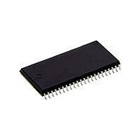
... Product Portfolio Product V Range (V) CC Min Typ CY62158ELL 4.5 5.0 Notes 1. NC pins are not connected on the die. 2. Typical values are included for reference only and are not guaranteed or tested. Typical values are measured at V Document #: 38-05684 Rev. *G Figure 1. 44-Pin TSOP II (Top View) ...
Page 4
... CMOS levels to meet the Document #: 38-05684 Rev Input Voltage Output Current into Outputs (LOW)............................. 20 mA Static Discharge Voltage............................................ >2001V (MIL-STD-883, Method 3015) Latch up Current...................................................... >200 mA Operating Range + 0.5V CC(max) Device + 0.5V CY62158ELL CC(max) Test Conditions I = – 2 4. 4.5V to 5.5V CC GND < ...
Page 5
OUTPUT R2 100 pF INCLUDING JIG AND SCOPE Parameters Data Retention Characteristics Over the Operating Range Parameter Description V V for Data Retention DR CC [8] I Data Retention Current CCDR ...
Page 6
... HZOE HZCE HZWE 14. The internal write time of the memory is defined by the overlap of WE, CE can terminate a write by going INACTIVE. The data input setup and hold timing should be referenced to the edge of the signal that terminates the write. Document #: 38-05684 Rev. *G Description ...
Page 7
Switching Waveforms Figure 4 shows address transition controlled read cycle waveforms. ADDRESS PREVIOUS DATA VALID DATA OUT Figure 5 shows OE controlled read cycle waveforms. ADDRESS ACE OE t LZOE HIGH IMPEDANCE DATA OUT t ...
Page 8
... DATA I/O Notes 18. The internal write time of the memory is defined by the overlap of WE, CE can terminate a write by going INACTIVE. The data input setup and hold timing should be referenced to the edge of the signal that terminates the write. 19. Data I/O is high impedance 20 goes HIGH or CE goes LOW simultaneously with WE HIGH, the output remains in high impedance state ...
Page 9
Switching Waveforms (continued) Figure 8 shows WE controlled, OE LOW write cycle waveforms. ADDRESS DATA I/O NOTE 21 t HZWE Truth Table [22 ...
Page 10
... Ordering Information Speed (ns) Ordering Code 45 CY62158ELL-45ZSXI Contact your local Cypress sales representative for availability of this part. Ordering Code Definitions 621 -xx xxx CY 8 Document #: 38-05684 Rev. *G Package Package Type Diagram 51-85087 44-Pin TSOP II (Pb-free) I Temperature Grade Industrial Package Type: ZSX = VFBGA (Pb-free) ...
Page 11
Package Diagrams 22 23 TOP VIEW 0.400(0.016) 0.800 BSC 0.300 (0.012) (0.0315) 18.517 (0.729) 18.313 (0.721) DIMENSION IN MM (INCH) MAX MIN. Document #: 38-05684 Rev. *G Figure 9. 44-Pin TSOP II, 51-85087 PIN 1 I. BASE PLANE ...
Page 12
Document History Page Document Title: CY62158E MoBL 8-Mbit ( Static RAM Document Number: 38-05684 REV. ECN NO. Issue Date ** 270350 See ECN *A 291271 See ECN *B 1462592 See ECN VKN/AESA Converted from preliminary to final ...
Page 13
... Cypress against all charges. Any Source Code (software and/or firmware) is owned by Cypress Semiconductor Corporation (Cypress) and is protected by and subject to worldwide patent protection (United States and foreign), United States copyright laws and international treaty provisions. Cypress hereby grants to licensee a personal, non-exclusive, non-transferable license to copy, use, modify, create derivative works of, and compile the Cypress Source Code and derivative works for the sole purpose of creating custom software and or firmware in support of licensee product to be used only in conjunction with a Cypress integrated circuit as specified in the applicable agreement ...