CY62146ELL-45ZSXI Cypress Semiconductor Corp, CY62146ELL-45ZSXI Datasheet - Page 5
CY62146ELL-45ZSXI
Manufacturer Part Number
CY62146ELL-45ZSXI
Description
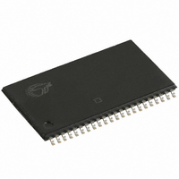
IC SRAM 4MBIT 45NS 44TSOP
Manufacturer
Cypress Semiconductor Corp
Type
Asynchronousr
Datasheet
1.CY62146ELL-45ZSXI.pdf
(14 pages)
Specifications of CY62146ELL-45ZSXI
Memory Size
4M (256K x 16)
Package / Case
44-TSOP II
Format - Memory
RAM
Memory Type
SRAM
Speed
45ns
Interface
Parallel
Voltage - Supply
4.5 V ~ 5.5 V
Operating Temperature
-40°C ~ 85°C
Access Time
45 ns
Supply Voltage (max)
5.5 V
Supply Voltage (min)
4.5 V
Maximum Operating Current
20 mA
Maximum Operating Temperature
+ 85 C
Minimum Operating Temperature
- 40 C
Mounting Style
SMD/SMT
Number Of Ports
1
Operating Supply Voltage
5 V
Density
4Mb
Access Time (max)
45ns
Sync/async
Asynchronous
Architecture
Not Required
Clock Freq (max)
Not RequiredMHz
Operating Supply Voltage (typ)
5V
Address Bus
18b
Package Type
TSOP-II
Operating Temp Range
-40C to 85C
Supply Current
20mA
Operating Supply Voltage (min)
4.5V
Operating Supply Voltage (max)
5.5V
Operating Temperature Classification
Industrial
Mounting
Surface Mount
Pin Count
44
Word Size
16b
Number Of Words
256K
Memory Configuration
256K X 16
Supply Voltage Range
4.5V To 5.5V
Memory Case Style
TSOP
No. Of Pins
44
Operating Temperature Range
-40°C To +85°C
Rohs Compliant
Yes
Lead Free Status / RoHS Status
Lead free / RoHS Compliant
Lead Free Status / RoHS Status
Lead free / RoHS Compliant, Lead free / RoHS Compliant
Other names
428-2070
CY62146ELL-45ZSXI
CY62146ELL-45ZSXI
Available stocks
Company
Part Number
Manufacturer
Quantity
Price
Company:

Part Number:
CY62146ELL-45ZSXI
Manufacturer:
WESTCODE
Quantity:
1 200


Data Retention Characteristics
Over the Operating Range
Notes
Document Number: 001-07970 Rev. *G
V
I
t
t
9. Typical values are included for reference only and are not guaranteed or tested. Typical values are measured at V
10. Chip enable (CE) and byte enables (BHE and BLE) need to be tied to CMOS levels to meet the I
11. Tested initially and after any design or process changes that may affect these parameters.
12. Full device operation requires linear V
CCDR
CDR
R
Parameter
DR
[12]
[11]
[10]
V
CE
CC
V
Data retention current
Chip deselect to data
retention time
Operation recovery time
CC
Parameters
OUTPUT
for data retention
INCLUDING
R
V
V
R1
R2
SCOPE
JIG AND
TH
TH
CC
Description
30 pF
R1
CC
ramp from V
R2
V
Figure 2. AC Test Loads and Waveforms
V
V
t
CC(min)
CDR
DR
CC
IN
Figure 3. Data Retention Waveform
to V
Rise Time = 1 V/ns
> V
= 2 V, CE > V
CC(min)
CC
– 0.2 V or V
> 100 s or stable at V
GND
V
CC
Equivalent to:
Conditions
DATA RETENTION MODE
CC
5.0 V
1800
1.77
990
639
10%
– 0.2 V,
IN
OUTPUT
< 0.2 V
V
DR
> 2.0 V
ALL INPUT PULSES
CC(min)
90%
THÉ VENIN EQUIVALENT
SB2
> 100 s.
/ I
CCDR
spec. Other inputs are left floating.
R
TH
Min
45
CC
90%
2
–
0
= V
10%
V
Fall Time = 1 V/ns
CC(typ)
CC(min)
V
t
R
TH
CY62146E MoBL
Typ
, T
–
1
–
–
A
[9]
= 25 °C.
Unit
V
Max
–
7
–
–
Page 5 of 14
Unit
A
ns
ns
V
[+] Feedback
Related parts for CY62146ELL-45ZSXI
Image
Part Number
Description
Manufacturer
Datasheet
Request
R

Part Number:
Description:
CY62146ELL-45ZSXIT
Manufacturer:
Cypress Semiconductor Corp
Datasheet:
Part Number:
Description:
CY62146ELL-45ZSXAT
Manufacturer:
Cypress Semiconductor Corp
Datasheet:
Part Number:
Description:
IC SRAM 4MBIT 45NS 44TSOP
Manufacturer:
Cypress Semiconductor Corp
Datasheet:

Part Number:
Description:
Manufacturer:
Cypress Semiconductor Corp
Datasheet:
Part Number:
Description:
Manufacturer:
Cypress Semiconductor Corp
Datasheet:
Part Number:
Description:
Manufacturer:
Cypress Semiconductor Corp
Datasheet:
Part Number:
Description:
Manufacturer:
Cypress Semiconductor Corp
Datasheet: