CY7C1041D-10VXI Cypress Semiconductor Corp, CY7C1041D-10VXI Datasheet

IC SRAM 4MBIT 10NS 44SOJ

CY7C1041D-10VXI

Manufacturer Part Number
CY7C1041D-10VXI
Description
IC SRAM 4MBIT 10NS 44SOJ
Manufacturer
Cypress Semiconductor Corp
Type
Asynchronousr
Datasheet

Specifications of CY7C1041D-10VXI

Memory Size
4M (256K x 16)
Package / Case
44-SOJ
Format - Memory
RAM
Memory Type
SRAM - Asynchronous
Speed
10ns
Interface
Parallel
Voltage - Supply
4.5 V ~ 5.5 V
Operating Temperature
-40°C ~ 85°C
Access Time
10 ns
Supply Voltage (max)
5.5 V
Supply Voltage (min)
4.5 V
Maximum Operating Current
90 mA
Maximum Operating Temperature
+ 85 C
Minimum Operating Temperature
- 40 C
Mounting Style
SMD/SMT
Number Of Ports
1
Operating Supply Voltage
5 V
Density
4Mb
Access Time (max)
10ns
Sync/async
Asynchronous
Architecture
Not Required
Clock Freq (max)
Not RequiredMHz
Operating Supply Voltage (typ)
5V
Address Bus
18b
Package Type
SOJ
Operating Temp Range
-40C to 85C
Supply Current
90mA
Operating Supply Voltage (min)
4.5V
Operating Supply Voltage (max)
5.5V
Operating Temperature Classification
Industrial
Mounting
Surface Mount
Pin Count
44
Word Size
16b
Number Of Words
256K
Memory Configuration
256K X 16
Supply Voltage Range
4.5V To 5.5V
Memory Case Style
SOJ
No. Of Pins
44
Operating Temperature Range
-40°C To +85°C
Rohs Compliant
Yes
Lead Free Status / RoHS Status
Lead free / RoHS Compliant
Lead Free Status / RoHS Status
Lead free / RoHS Compliant, Lead free / RoHS Compliant
Other names
428-1975-5
CY7C1041D-10VXI
Cypress Semiconductor Corporation
Document #: 38-05472 Rev. *E
Features
Note:
1. For guidelines on SRAM system design, please refer to the “System Design Guidelines” Cypress application note, available on the internet at www.cypress.com.
• Pin-and function-compatible with CY7C1041B
• High speed
• Low active power
• Low CMOS standby power
• 2.0 V Data Retention
• Automatic power-down when deselected
• TTL-compatible inputs and outputs
• Easy memory expansion with CE and OE features
• Available in lead-free 44-Lead (400-Mil) Molded SOJ and
A
A
A
A
A
A
A
A
A
Logic Block Diagram
— t
— I
— I
44-Pin TSOP II packages
0
1
2
3
4
5
6
7
8
CC
SB2
AA
= 90 mA at 10 ns (Industrial)
= 10 ns
= 10 mA
INPUT BUFFER
DECODER
COLUMN
256K x 16
198 Champion Court
I/O
I/O
0
8
–I/O
–I/O
BHE
WE
CE
OE
BLE
Functional Description
The CY7C1041D is a high-performance CMOS static RAM
organized as 256K words by 16 bits. Writing to the device is
accomplished by taking Chip Enable (CE) and Write Enable
(WE) inputs LOW. If Byte Low Enable (BLE) is LOW, then data
from I/O pins (I/O
specified on the address pins (A
Enable (BHE) is LOW, then data from I/O pins (I/O
I/O
(A
Reading from the device is accomplished by taking Chip
Enable (CE) and Output Enable (OE) LOW while forcing the
Write Enable (WE) HIGH. If Byte Low Enable (BLE) is LOW,
then data from the memory location specified by the address
pins will appear on I/O
LOW, then data from memory will appear on I/O
the truth table at the back of this data sheet for a complete
description of read and write modes.
The input/output pins (I/O
high-impedance state when the device is deselected (CE
HIGH), the outputs are disabled (OE HIGH), the BHE and BLE
are disabled (BHE, BLE HIGH), or during a write operation (CE
LOW, and WE LOW).
The CY7C1041D is available in a standard 44-pin
400-mil-wide body width SOJ and 44-pin TSOP II package
with center power and ground (revolutionary) pinout.
7
15
4-Mbit (256K x 16) Static RAM
0
15
through A
) is written into the location specified on the address pins
San Jose
17
).
0
through I/O
,
Pin Configurations
I/O
I/O
I/O
I/O
V
I/O
I/O
I/O
I/O
V
WE
CE
CA 95134-1709
CC
A
A
A
A
A
0
A
A
A
A
A
SS
5
6
7
8
9
0
1
2
3
4
0
1
2
3
4
5
6
7
to I/O
SOJ / TSOPII
0
13
14
15
16
17
18
19
20
21
22
Top View
1
2
3
4
5
6
7
8
9
10
11
12
through I/O
[1]
7
. If Byte High Enable (BHE) is
7
), is written into the location
Revised December 13, 2010
0
through A
44
43
42
41
40
39
38
37
36
35
34
33
32
31
30
29
28
27
26
25
24
23
A
A
A
OE
BHE
BLE
I/O
I/O
I/O
I/O
V
V
I/O
I/O
I/O
I/O
NC
A
A
A
A
A
17
16
15
SS
CC
14
13
12
11
10
15
CY7C1041D
15
14
13
12
11
10
9
8
) are placed in a
17
). If Byte High
8
408-943-2600
to I/O
8
through
15
. See
[+] Feedback

Related parts for CY7C1041D-10VXI

CY7C1041D-10VXI Summary of contents

Page 1

... Document #: 38-05472 Rev. *E 4-Mbit (256K x 16) Static RAM Functional Description The CY7C1041D is a high-performance CMOS static RAM organized as 256K words by 16 bits. Writing to the device is accomplished by taking Chip Enable (CE) and Write Enable (WE) inputs LOW. If Byte Low Enable (BLE) is LOW, then data ...

Page 2

... CE > > < MAX , CE > V – 0.3V > V – 0.3V < 0.3V Test Conditions T = 25 MHz 5.0V CC CY7C1041D [2] Unit Ambient Temperature V Speed CC 5V  0.5 –40C to +85  0.5 –40C to +125 -12 (Automotive) Max. Min. Max. Unit 2.4 V 0.4 ...

Page 3

... CC is less than less than less than t HZCE LZCE HZOE LZOE HZBE CY7C1041D SOJ Package TSOP II Package Unit C/W 57.91 50.66 C/W 36.73 17.17 ALL INPUT PULSES 90% 90% 10% 10%  (b) THÉ VENIN EQUIVALENT 167 ...

Page 4

... Over the Operating Range [13] Conditions 2.0V > V – 0.3V > V – 0. < 0. DATA RETENTION MODE 4.5V V > CDR OHA and t HZWE > 50 s or stable at V > 50  CC(min.) CC(min CY7C1041D -12 (Automotive) Max. Min. Max. Unit Min. Max. Unit 2.0 V Ind’ Auto ...

Page 5

... Address valid prior to or coincident with CE transition LOW 17. Data I/O is high impedance BHE and/or BLE goes HIGH simultaneously with WE going HIGH, the output remains in a high-impedance state. Document #: 38-05472 Rev DOE DATA VALID 50 SCE PWE CY7C1041D t HZOE t HZCE t HZBE HIGH IMPEDANCE Page ICC ISB ...

Page 6

... Write Cycle No. 3 (WE Controlled, OE HIGH During Write) ADDRESS BHE, BLE DATA I/O NOTE 19 t HZOE Note: 19. During this period the I/Os are in the output state and input signals should not be applied. Document #: 38-05472 Rev PWE t SCE t SD [16, 17 SCE PWE t SD DATA VALID IN CY7C1041D Page [+] Feedback ...

Page 7

... Power Down Data Out Read All bits High Z Read Lower bits only Data Out Read Upper bits only Data In Write All bits High Z Write Lower bits only Data In Write Upper bits only High Z Selected, Outputs Disabled CY7C1041D LZWE Mode Power Standby ( Active ( ...

Page 8

... Cypress maintains a worldwide network of offices, solution centers, manufacturer's representatives and distributors. To find the office closest to you, visit us at http://www.cypress.com/go/datasheet/offices. Speed (ns) Ordering Code 10 CY7C1041D-10VXI 51-85082 CY7C1041D-10ZSXI 51-85087 Ordering Code Definitions CY 7 ...

Page 9

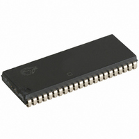
... Package Diagrams Figure 1. 44-Lead (400-Mil) Molded SOJ (51-85082) All products and company names mentioned in this document may be the trademarks of their respective holders. Document #: 38-05472 Rev. *E Figure 2. 44-pin TSOP II (51-85087) CY7C1041D 51-85082 *C 51-85087 *B 51-85087 *C Page [+] Feedback ...

Page 10

... Document History Page Document Title: CY7C1041D 4-Mbit (256K x 16) Static RAM Document Number: 38-05472 Orig. of REV. ECN NO. Issue Date Change ** 201560 See ECN *A 233729 See ECN *B 351117 See ECN *C 446328 See ECN *D 2897049 03/22/10 *E 3109184 12/13/2010 Document #: 38-05472 Rev. *E Description of Change ...

Page 11

... The inclusion of Cypress products in life-support systems application implies that the manufacturer assumes all risk of such use and in doing so indemnifies Cypress against all charges. cypress.com/go/plc CY7C1041D PSoC Solutions psoc.cypress.com/solutions ...

Related keywords