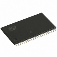
CY7C1021CV26-15ZSXE Cypress Semiconductor Corp, CY7C1021CV26-15ZSXE Datasheet - Page 5

CY7C1021CV26-15ZSXE
Manufacturer Part Number
CY7C1021CV26-15ZSXE
Description
IC SRAM 1MBIT 15NS 44TSOP
Manufacturer
Cypress Semiconductor Corp
Type
Asynchronousr
Datasheet
1.CY7C1021CV26-15ZSXE.pdf
(15 pages)
Specifications of CY7C1021CV26-15ZSXE
Memory Size
1M (64K x 16)
Package / Case
44-TSOP II
Format - Memory
RAM
Memory Type
SRAM - Asynchronous
Speed
15ns
Interface
Parallel
Voltage - Supply
2.5 V ~ 2.7 V
Operating Temperature
-40°C ~ 125°C
Access Time
15 ns
Supply Voltage (max)
2.7 V
Supply Voltage (min)
2.5 V
Maximum Operating Current
80 mA
Maximum Operating Temperature
+ 125 C
Minimum Operating Temperature
- 40 C
Mounting Style
SMD/SMT
Number Of Ports
1
Lead Free Status / RoHS Status
Lead free / RoHS Compliant
Lead Free Status / RoHS Status
Lead free / RoHS Compliant, Lead free / RoHS Compliant
AC Test Loads and Waveforms
Switching Characteristics
Over the Operating Range
Document Number: 38-05589 Rev. *E
Read Cycle
t
t
t
t
t
t
t
t
t
t
t
t
t
t
Notes
RC
AA
OHA
ACE
DOE
LZOE
HZOE
LZCE
HZCE
PU
PD
DBE
LZBE
HZBE
5. AC characteristics (except high Z) are tested using the Thevenin load shown in Figure (a). High Z characteristics are tested for all speeds using the test load
6. Test conditions assume signal transition time of 2.6 ns or less, timing reference levels of 1.3 V, input pulse levels of 0 to 2.6 V.
7. At any given temperature and voltage condition, t
8. t
9. This parameter is guaranteed by design and is not tested.
OUTPUT
[9]
[9]
Parameter
2.6 V
shown in Figure (c)
HZOE
JIG AND
SCOPE
INCLUDING
, t
HZBE
30 pF
, t
HZCE
, and t
1830
(a)
R1
Read cycle time
Address to data valid
Data hold from address change
CE LOW to data valid
OE LOW to data valid
OE LOW to low Z
OE HIGH to high Z
CE LOW to low Z
CE HIGH to high Z
CE LOW to power-up
CE HIGH to power-down
Byte enable to data valid
Byte enable to low Z
Byte disable to high Z
HZWE
1976
R2
[6]
are specified with a load capacitance of 5 pF as in part (d) of AC Test Loads. Transition is measured 500 mV from steady-state voltage.
2.6V
GND
Rise Time: 1 V/ns
[7]
[7]
[7, 8]
Description
[7, 8]
HZCE
[5]
is less than t
10%
90%
LZCE
ALL INPUT PULSES
, t
HZOE
(b)
is less than t
Fall Time: 1 V/ns
90%
LZOE
10%
, and t
HZWE
Min
15
–
3
–
–
0
–
3
–
0
–
–
0
–
High Z characteristics:
is less than t
OUTPUT
–15
LZWE
2.6V
for any given device.
Max
5 pF
15
15
15
–
–
7
–
7
–
7
–
7
–
7
CY7C1021CV26
R 317
(c)
Page 5 of 15
Unit
351
ns
ns
ns
ns
ns
ns
ns
ns
ns
ns
ns
ns
ns
ns
R2
[+] Feedback


