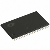
CY7C1021CV26-15ZSXE Cypress Semiconductor Corp, CY7C1021CV26-15ZSXE Datasheet

CY7C1021CV26-15ZSXE
Specifications of CY7C1021CV26-15ZSXE
Related parts for CY7C1021CV26-15ZSXE
CY7C1021CV26-15ZSXE Summary of contents
Page 1
... CMOS for optimum speed/power ■ Available in Pb-free and non Pb-free 44-pin TSOP II , 44-pin ■ (400-Mil) Molded SOJ and Pb-free 48-ball FPBGA packages Functional Description The CY7C1021CV26 is a high-performance CMOS static RAM organized as 65,536 words by 16 bits. This device has Logic Block Diagram ...
Page 2
... AC Test Loads and Waveforms ....................................... 5 Switching Characteristics ................................................ 5 Switching Waveforms ...................................................... 7 Read Cycle No. 1 ........................................................ 7 Read Cycle No. 2 (OE Controlled) .............................. 7 Write Cycle No. 1 (CE Controlled) ............................... 8 Document Number: 38-05589 Rev. *E CY7C1021CV26 Write Cycle No. 2 (BLE or BHE Controlled) ................ 8 Write Cycle No. 3 (WE Controlled, LOW) .................... 9 Truth Table ........................................................................ 9 Ordering Information ...................................................... 10 Ordering Code Definitions ......................................... 10 Package Diagrams .......................................................... 11 Acronyms ...
Page 3
... Output Enable, active LOW. Controls the direction of the I/O pins. When LOW, the I/O pins are allowed to behave as outputs. When deasserted HIGH, I/O pins are tri-stated, and act as input data pins. Ground for the device. Should be connected to ground of the system. Power Supply inputs to the device. CY7C1021CV26 Unit – ...
Page 4
... Max > > Max > V – 0 > < 0 Test Conditions = 25 MHz 2 Test Conditions four-layer printed circuit board CY7C1021CV26 [3] ............................... –0 0 Ambient V CC Temperature –40 C to +125 C 2.5 V–2.7 V –15 Unit Min Max 2.3 – – 0.4 2 0.3 CC –0.3 0.8 –3 +3 –3 ...
Page 5
... Fall Time: 1 V/ns (b) Min 15 – 3 – – 0 – 3 – 0 – – 0 – is less than less than t , and t HZCE LZCE HZOE LZOE HZWE CY7C1021CV26 High Z characteristics: R 317 2.6V OUTPUT 351 (c) –15 Unit Max – – – – – ...
Page 6
... HZOE HZBE HZCE HZWE Document Number: 38-05589 Rev. *E Min – less than less than t , and t HZCE LZCE HZOE LZOE HZWE CY7C1021CV26 –15 Unit Max – ns – ns – ns – ns – ns – ns – ns – ns – – less than t for any given device. ...
Page 7
... CURRENT Notes 13. Device is continuously selected. OE, CE, BHE and/or BLE = V 14 HIGH for Read cycle. 15. Address valid prior to or coincident with CE transition LOW. Document Number: 38-05589 Rev OHA [14, 15 DATA VALID 50 CY7C1021CV26 DATA VALID t HZOE t HZCE t HZBE HIGH IMPEDANCE ICC CC 50% I ISB SB ...
Page 8
... Write Cycle No. 2 (BLE or BHE Controlled) ADDRESS t SA BHE, BLE WE CE DATA I/O Notes 16. Data I/O is high-impedance BHE and/or BLE goes HIGH simultaneously with WE going HIGH, the output remains in a high-impedance state. Document Number: 38-05589 Rev. *E [16, 17 SCE PWE PWE t SCE CY7C1021CV26 Page [+] Feedback ...
Page 9
... Read – Lower bits only Data Out Read – Upper bits only Data In Write – All bits High Z Write – Lower bits only Data In Write – Upper bits only High Z Selected, Outputs Disabled High Z Selected, Outputs Disabled CY7C1021CV26 LZWE Mode Power Standby ( Active (I ...
Page 10
... Cypress maintains a worldwide network of offices, solution centers, manufacturer's representatives and distributors. To find the office closest to you, visit us at http://www.cypress.com/go/datasheet/offices. Speed (ns) Ordering Code 15 CY7C1021CV26-15ZSXE CY7C1021CV26-15VXE CY7C1021CV26-15BAE CY7C1021CV26-15BAET CY7C1021CV26-15VXET CY7C1021CV26-15ZSXET Ordering Code Definitions CY7C 1021 C V26 - 15 XXX E X Document Number: 38-05589 Rev. *E http://www.cypress.com/products or contact your local sales representative. Package ...
Page 11
... Package Diagrams Document Number: 38-05589 Rev. *E Figure 1. 44-pin TSOP II, 51-85087 51-85087 *C Figure 2. 44-pin (400-Mil) Molded SOJ, 51-85082 CY7C1021CV26 51-85087-*A 51-85082 *C Page [+] Feedback ...
Page 12
... Package Diagrams (continued) Figure 3. 48-ball FBGA (6 × 8 × 1 mm), 51-85150 Document Number: 38-05589 Rev. *E CY7C1021CV26 51-85150 *F Page [+] Feedback ...
Page 13
... J-lead SRAM static random access memory TSOP thin small-outline package TTL transistor-transistor logic FPBGA fine-pitch ball grid array WE write enable Document Number: 38-05589 Rev. *E CY7C1021CV26 Document Conventions Units of Measure Symbol Unit of Measure ns nano seconds V Volts µA micro Amperes mA milli Amperes ...
Page 14
... Document History Page Document Title: CY7C1021CV26 1-Mbit (64 K × 16) Static RAM Document Number: 38-05589 Orig. of REV. ECN NO. Issue Date Change ** 238454 See ECN *A 335861 See ECN *B 493543 See ECN *C 2897087 03/22/10 *D 3057593 10/13/2010 *E 3098812 12/01/2010 Document Number: 38-05589 Rev. *E Description of Change ...
Page 15
... Cypress against all charges. Use may be limited by and subject to the applicable Cypress software license agreement. Document Number: 38-05589 Rev. *E All products and company names mentioned in this document may be the trademarks of their respective holders. cypress.com/go/plc Revised December 1, 2010 CY7C1021CV26 PSoC Solutions psoc.cypress.com/solutions PSoC 1 | PSoC 3 ...


