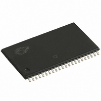
CY7C1020CV26-15ZSXE Cypress Semiconductor Corp, CY7C1020CV26-15ZSXE Datasheet

CY7C1020CV26-15ZSXE
Specifications of CY7C1020CV26-15ZSXE
Related parts for CY7C1020CV26-15ZSXE
CY7C1020CV26-15ZSXE Summary of contents
Page 1
... CMOS for optimum speed and power ■ Package offered: 44-pin TSOP II ■ Functional Description The CY7C1020CV26 is a high performance CMOS static RAM organized as 32,768 words by 16 bits. This device has an automatic power down feature that significantly reduces power consumption when deselected. Logic Block Diagram Cypress Semiconductor Corporation Document #: 38-05406 Rev ...
Page 2
... Pin Configuration Selection Guide Description Maximum Access Time Maximum Operating Current Maximum CMOS Standby Current Document #: 38-05406 Rev. *C Figure 1. 44-Pin TSOP II (Top View) CY7C1020CV26-15 15 100 5 CY7C1020CV26 Unit Page [+] Feedback ...
Page 3
... CC CE > V – 0.3V, V > V – 0.3V < 0.3V Test Conditions T = 25 MHz 2.6V CC CY7C1020CV26 [1] .................................. –0. +0.5V CC Ambient V CC Temperature –40C to +125C 2.5V to 2.7V CY7C1020CV26 Unit Min Max 2.3 V 0 –0.3 0.8 V A –5 +5 A –5 +5 –300 mA 100 ...
Page 4
... Figure 2. AC Test Loads and Waveforms R 1830 2.5V GND R2 1976 Rise Time: 1 V/ns (a) Over the Operating Range Description [5] [5, 6] [5] [5, 6] [5] [ less than less than t , and t LZCE HZOE LZOE HZWE CY7C1020CV26 [4] ALL INPUT PULSES 90% 90% 10% 10% Fall Time:1 V/ns (b) CY7C1020CV26 Unit Min Max ...
Page 5
... Device is continuously selected. OE, CE, BHE and/or BHE = V 10 HIGH for read cycle. 11. Address valid prior to or coincident with CE transition LOW. Document #: 38-05406 Rev. *C [9, 10] Figure 3. Read Cycle No OHA t RC DATA VALID 50 CY7C1020CV26 DATA VALID [10, 11] t HZOE t HZCE t HZBE HIGH IMPEDANCE ICC CC 50% I ...
Page 6
... Figure 6. Write Cycle No. 2 (BLE or BHE Controlled) ADDRESS t SA BHE, BLE WE CE DATA I/O Notes 12. Data I/O is high impedance BHE and BLE = V 13 goes HIGH simultaneously with WE going HIGH, the output remains in a high impedance state. Document #: 38-05406 Rev. *C [12, 13 SCE PWE PWE t SCE CY7C1020CV26 Page [+] Feedback ...
Page 7
... Read – Lower bits only Data Out Read – Upper bits only Data In Write – All bits High Z Write – Lower bits only Data In Write – Upper bits only High Z Selected, Outputs Disabled High Z Selected, Outputs Disabled CY7C1020CV26 LZWE Mode Power Standby ( Active (I ...
Page 8
... Ordering Information Speed (ns) Ordering Code 15 CY7C1020CV26-15ZSXE Ordering Code Definitions V26 - 15 ZSX Document #: 38-05406 Rev. *C Package Package Type Name Z44 44-pin TSOP Type II (Pb-free) E Temperature Range Automotive Package Type: ZSX = 44-pin TSOP Type II (Pb-free) Speed V26 = Voltage range (2 2 0.16 µm Technology 0 = Data width × ...
Page 9
... Package Diagrams Document #: 38-05406 Rev. *C Figure 8. 44-Pin TSOP II CY7C1020CV26 51-85087 *C Page [+] Feedback ...
Page 10
... Document History Page Document Title: CY7C1020CV26 512 Kb (32 K × 16) Static RAM Document Number: 38-05406 Submission REV. ECN NO. Date ** 128060 07/30/03 *A 352999 See ECN *B 2903127 04/01/2010 *C 3109992 12/14/2010 Document #: 38-05406 Rev. *C Orig. of Description of Change Change EJH Customized data sheet to meet special requirements for CG5988AF Automotive temperature range: – ...
Page 11
... Cypress against all charges. Use may be limited by and subject to the applicable Cypress software license agreement. Document #: 38-05406 Rev. *C All products and company names mentioned in this document may be the trademarks of their respective holders. cypress.com/go/plc Revised December 14, 2010 CY7C1020CV26 PSoC Solutions psoc.cypress.com/solutions PSoC 1 | PSoC 3 ...


