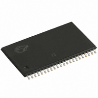
CY62126EV30LL-45ZSXI Cypress Semiconductor Corp, CY62126EV30LL-45ZSXI Datasheet - Page 9

CY62126EV30LL-45ZSXI
Manufacturer Part Number
CY62126EV30LL-45ZSXI
Description
IC SRAM 1MBIT 45NS 44TSOP
Manufacturer
Cypress Semiconductor Corp
Type
Asynchronousr
Datasheet
1.CY62126EV30LL-45ZSXI.pdf
(16 pages)
Specifications of CY62126EV30LL-45ZSXI
Memory Size
1M (64K x 16)
Package / Case
44-TSOP II
Format - Memory
RAM
Memory Type
SRAM
Speed
45ns
Interface
Parallel
Voltage - Supply
2.2 V ~ 3.6 V
Operating Temperature
-40°C ~ 85°C
Access Time
45 ns
Supply Voltage (max)
3.6 V
Supply Voltage (min)
2.2 V
Maximum Operating Current
16 mA
Organization
64 K x 16
Maximum Operating Temperature
+ 85 C
Minimum Operating Temperature
- 40 C
Mounting Style
SMD/SMT
Number Of Ports
1
Operating Supply Voltage
2.5 V or 3.3 V
Memory Configuration
64K X 16
Supply Voltage Range
2.2V To 3.6V
Memory Case Style
TSOP
No. Of Pins
44
Operating Temperature Range
-40°C To +85°C
Rohs Compliant
Yes
Lead Free Status / RoHS Status
Lead free / RoHS Compliant
Lead Free Status / RoHS Status
Lead free / RoHS Compliant, Lead free / RoHS Compliant
Other names
428-2063
CY62126EV30LL-45ZSXI
CY62126EV30LL-45ZSXI
Available stocks
Company
Part Number
Manufacturer
Quantity
Price
Company:
Part Number:
CY62126EV30LL-45ZSXI
Manufacturer:
INTEL
Quantity:
1 152
Part Number:
CY62126EV30LL-45ZSXI
Manufacturer:
CYPRESS
Quantity:
20 000
Switching Waveforms
Document #: 38-05486 Rev. *H
Notes
19. The internal write time of the memory is defined by the overlap of WE, CE = V
20. Data I/O is high impedance if OE = V
21. If CE goes high simultaneously with WE = V
22. During this period, the I/Os are in output state. Do not apply input signals.
ADDRESS
ADDRESS
these signals can terminate a write by going inactive. The data input setup and hold timing must refer to the edge of signal that terminates write.
BHE/BLE
BHE/BLE
DATA I/O
DATA I/O
WE
WE
OE
OE
CE
CE
NOTE 22
NOTE 22
(continued)
IH
.
t
HZOE
t
Figure 8. Write Cycle No. 2 (CE controlled)
Figure 7. Write Cycle No. 1 (WE controlled)
SA
t
HZOE
IH
, the output remains in a high impedance state.
t
SA
t
AW
t
AW
t
t
SCE
WC
t
IL
WC
, BHE, BLE or both = V
t
BW
t
BW
DATA
t
t
PWE
SD
DATA
t
t
PWE
SD
t
IN
SCE
IN
[
19
[19, 20, 21]
IL
, 20, 21]
. All signals must be active to initiate a write and any of
t
HD
CY62126EV30 MoBL
t
HA
t
HA
t
HD
Page 9 of 16


