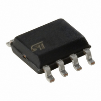
M95M01-RMN6TP STMicroelectronics, M95M01-RMN6TP Datasheet - Page 21

M95M01-RMN6TP
Manufacturer Part Number
M95M01-RMN6TP
Description
IC EEPROM 1MBIT 5MHZ 8SOIC
Manufacturer
STMicroelectronics
Datasheet
1.M95M01-RMN6TP.pdf
(41 pages)
Specifications of M95M01-RMN6TP
Format - Memory
EEPROMs - Serial
Memory Type
EEPROM
Memory Size
1M (128K x 8)
Speed
5MHz
Interface
SPI, 3-Wire Serial
Voltage - Supply
1.8 V ~ 5.5 V
Operating Temperature
-40°C ~ 85°C
Package / Case
8-SOIC (3.9mm Width)
Organization
128 K x 8
Interface Type
SPI
Maximum Clock Frequency
5 MHz
Access Time
80 ns
Supply Voltage (max)
5.5 V
Supply Voltage (min)
1.8 V
Maximum Operating Current
5 mA
Maximum Operating Temperature
+ 85 C
Mounting Style
SMD/SMT
Minimum Operating Temperature
- 40 C
Operating Supply Voltage
2.5 V, 3.3 V, 5 V
Lead Free Status / RoHS Status
Lead free / RoHS Compliant
Other names
497-8701-2
M95M01-RMN6TP
M95M01-RMN6TP
Available stocks
Company
Part Number
Manufacturer
Quantity
Price
Company:
Part Number:
M95M01-RMN6TP
Manufacturer:
INFINEON
Quantity:
23
Company:
Part Number:
M95M01-RMN6TP
Manufacturer:
STMicroelectronics
Quantity:
76 802
Part Number:
M95M01-RMN6TP
Manufacturer:
ST
Quantity:
20 000
M95M01-R, M95M01-W
Table 5.
1. As defined by the values in the Block Protect (BP1, BP0) bits of the Status Register, as shown in
The Write Status Register (WRSR) instruction allows the user to change the values of the
Block Protect (BP1, BP0) bits, to define the size of the area that is to be treated as read-
only, as defined in
The Write Status Register (WRSR) instruction also allows the user to set or reset the Status
Register Write Disable (SRWD) bit in accordance with the Write Protect (W) signal. The
Status Register Write Disable (SRWD) bit and Write Protect (W) signal allow the device to
be put in the Hardware Protected Mode (HPM). The Write Status Register (WRSR)
instruction is not executed once the Hardware Protected Mode (HPM) is entered.
The contents of the Status Register Write Disable (SRWD) and Block Protect (BP1, BP0)
bits are frozen at their current values from just before the start of the execution of Write
Status Register (WRSR) instruction. The new, updated, values take effect at the moment of
completion of the execution of Write Status Register (WRSR) instruction.
The protection features of the device are summarized in
When the Status Register Write Disable (SRWD) bit of the Status Register is 0 (its initial
delivery state), it is possible to write to the Status Register provided that the Write Enable
Latch (WEL) bit has previously been set by a Write Enable (WREN) instruction, regardless
of the whether Write Protect (W) is driven high or low.
When the Status Register Write Disable (SRWD) bit of the Status Register is set to 1, two
cases need to be considered, depending on the state of Write Protect (W):
●
●
Signal
W
1
0
1
0
If Write Protect (W) is driven high, it is possible to write to the Status Register provided
that the Write Enable Latch (WEL) bit has previously been set by a Write Enable
(WREN) instruction.
If Write Protect (W) is driven low, it is not possible to write to the Status Register even if
the Write Enable Latch (WEL) bit has previously been set by a Write Enable (WREN)
instruction. (Attempts to write to the Status Register are rejected, and are not accepted
for execution). As a consequence, all the data bytes in the memory area that are
software protected (SPM) by the Block Protect (BP1, BP0) bits of the Status Register,
are also hardware protected against data modification.
SRWD
Bit
0
0
1
1
Protection modes
Protected
Hardware
Protected
Software
(SPM)
(HPM)
Mode
Table
4.
Status Register is Writable
(if the WREN instruction
has set the WEL bit)
The values in the BP1 and
BP0 bits can be changed
Status Register is
Hardware write protected
The values in the BP1 and
BP0 bits cannot be
changed
Write Protection of the
Doc ID 13264 Rev 7
Status Register
Write Protected
Write Protected
Protected area
Table
2.
Memory content
(1)
Unprotected area
Ready to accept
Write instructions
Ready to accept
Write instructions
Instructions
Table
5.
21/41
(1)


