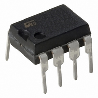
M24C32-WBN6P STMicroelectronics, M24C32-WBN6P Datasheet - Page 26

M24C32-WBN6P
Manufacturer Part Number
M24C32-WBN6P
Description
IC EEPROM 32KBIT 400KHZ 8DIP
Manufacturer
STMicroelectronics
Specifications of M24C32-WBN6P
Format - Memory
EEPROMs - Serial
Memory Type
EEPROM
Memory Size
32K (4K x 8)
Speed
400kHz
Interface
I²C, 2-Wire Serial
Voltage - Supply
2.5 V ~ 5.5 V
Operating Temperature
-40°C ~ 85°C
Package / Case
8-DIP (0.300", 7.62mm)
Organization
4 K x 8
Interface Type
I2C
Maximum Clock Frequency
0.4 MHz
Access Time
900 ns
Supply Voltage (max)
5.5 V
Supply Voltage (min)
2.5 V
Maximum Operating Current
2 mA
Maximum Operating Temperature
+ 85 C
Mounting Style
Through Hole
Minimum Operating Temperature
- 40 C
Operating Supply Voltage
2.5 V, 5.5 V
Memory Configuration
4096 X 8
Clock Frequency
400kHz
Supply Voltage Range
2.5V To 5.5V
Memory Case Style
DIP
No. Of Pins
8
Rohs Compliant
Yes
Lead Free Status / RoHS Status
Lead free / RoHS Compliant
Other names
497-8571
M24C32-WBN6P
M24C32-WBN6P
Available stocks
Company
Part Number
Manufacturer
Quantity
Price
DC and AC parameters
26/42
Table 12.
1. Only for devices operating at f
2. Characterized value, not tested in production.
3. The device is not selected after power-up, after a Read instruction (after the Stop condition), or after the
4. The new M24C32-W devices (identified by the process letter K) offer I
Symbol
I
I
V
I
V
I
CC0
CC1
V
completion of the internal write cycle t
I
CC
LO
LI
OL
IH
IL
Input leakage current
(SCL, SDA, E0, E1,
E2)
Output leakage
current
Supply current (Read)
Supply current (Write) During t
Standby supply
current
Input low voltage
(SCL, SDA, WC)
Input high voltage
(SCL, SDA)
Input high voltage
(WC, E0, E1, E2)
Output low voltage
DC characteristics (M24xxx-W, device grade 6)
Parameter
C
max = 1 MHz (see
Doc ID 4578 Rev 18
V
device in Standby mode
SDA in Hi-Z, external voltage applied
on SDA: V
2.5 V < V
(rise/fall time < 50 ns)
2.5 V < V
(rise/fall time < 50 ns)
Device not selected
V
Device not selected
V
I
I
OL
OL
IN
CC
CC
Test conditions (see
W
= 2.1 mA, V
= 3 mA, V
= V
, V
, V
(t
W
CC
CC
SS
W
is triggered by the correct decoding of a Write instruction).
CC
CC
, 2.5 V < V
= 2.5 V
= 5.5 V
or V
SS
< 5.5 V, f
< 5.5 V, f
M24C32-DF, M24C32-W, M24C32-R, M24C32-F
or V
CC
CC
Table
Table
CC
= 5.5 V
CC
= 2.5 V or
(3)
(3)
CC
17)
10)
c
c
, V
, V
= 400 kHz
= 1 MHz
< 5.5 V
IN
IN
Table 7
= V
= V
SS
SS
(1)
CC1
and
or
or
= 3µA (max)
0.7V
0.7V
–0.45
Min.
CC
CC
V
0.3V
CC
Max.
5
5
± 2
± 2
2.5
6.5
0.4
2
2
(2)
(4)
+0.6
CC
Unit
mA
mA
mA
µA
µA
µA
µA
V
V
V


