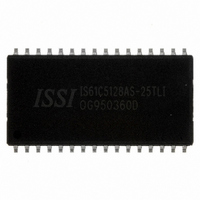
IS61C5128AS-25TLI ISSI, Integrated Silicon Solution Inc, IS61C5128AS-25TLI Datasheet
IS61C5128AS-25TLI
Specifications of IS61C5128AS-25TLI
Available stocks


Related parts for IS61C5128AS-25TLI


IS61C5128AS-25TLI Summary of contents
Page 1
... CMOS input levels. Easy memory expansion is provided by using Chip Enable and Output Enable inputs, CE and OE. The active LOW Write Enable (WE) controls both writing and reading of the memory. A data byte allows Upper Byte (UB) and Lower Byte (LB) access. The IS61C5128AL/AS and IS64C5128AL/AS are packaged ...
Page 2
IS61C5128AL/AS IS64C5128AL/AS HIGH SPEED (IS61/64C5128AL) PIN CONFIGURATION 36-Pin SOJ (400-mil I/ I/ GND 10 ...
Page 3
IS61C5128AL/AS IS64C5128AL/AS LOW POWER (IS61/64C5128AS) PIN CONFIGURATION 32-pin sTSOP (TYPE I) A11 A13 A18 6 A15 A17 9 A16 10 A14 11 A12 ...
Page 4
IS61C5128AL/AS IS64C5128AL/AS TRUTH TABLE Mode Not Selected X H Output Disabled H L Read H L Write L L ABSOLUTE MAXIMUM RATINGS Symbol Parameter V Terminal Voltage with Respect to ...
Page 5
IS61C5128AL/AS IS64C5128AL/AS OPERATING RANGE: HIGH SPEED OPTION (IS61/64C5128AL) Range Ambient Temperature Commercial 0°C to +70°C Industrial -40°C to +85°C Automotive -40°C to +125°C OPERATING RANGE: LOW POWER OPTION (IS61/64C5128AS) Range Ambient Temperature Commercial 0°C to +70°C Industrial -40°C to +85°C ...
Page 6
IS61C5128AL/AS IS64C5128AL/AS HIGH SPEED OPTION (IS61/64C5128AL) POWER SUPPLY CHARACTERISTICS Symbol Parameter Test Conditions I V Operating Supply Current I OUT I V Dynamic Operating Supply Current I OUT I TTL ...
Page 7
IS61C5128AL/AS IS64C5128AL/AS READ CYCLE SWITCHING CHARACTERISTICS Symbol Parameter t Read Cycle Time RC t Address Access Time AA t Output Hold Time OHA CE Access Time t ACE OE Access Time t DOE OE to High-Z Output t (2) HZOE ...
Page 8
IS61C5128AL/AS IS64C5128AL/AS AC WAVEFORMS (1,2) READ CYCLE NO. 1 ADDRESS D OUT PREVIOUS DATA VALID (1,3) READ CYCLE NO. 2 ADDRESS LZCS HIGH-Z D OUT Notes HIGH for a Read Cycle. 2. The device ...
Page 9
IS61C5128AL/AS IS64C5128AL/AS WRITE CYCLE SWITCHING CHARACTERISTICS Symbol Parameter t Write Cycle Time Write End t SCE t Address Setup Time AW to Write End t Address Hold from Write End HA t Address Setup Time SA WE ...
Page 10
IS61C5128AL/AS IS64C5128AL/AS AC WAVEFORMS WE Controlled WRITE CYCLE NO. 1 (WE ADDRESS DATA UNDEFINED OUT D IN Notes: 1. The internal write time is defined by the overlap of CE LOW and ...
Page 11
IS61C5128AL/AS IS64C5128AL/AS WRITE CYCLE NO. 2 (OE is HIGH During Write Cycle) ADDRESS OE CE LOW DATA UNDEFINED OUT D IN WRITE CYCLE NO. 3 (OE is LOW During Write Cycle) ADDRESS OE LOW CE LOW ...
Page 12
IS61C5128AL/AS IS64C5128AL/AS DATA RETENTION SWITCHING CHARACTERISTICS (HIGH SPEED) (IS61/64C5128AL) Symbol Parameter V V for Data Retention Data Retention Current DR t Data Retention Setup Time SDR t Recovery Time RDR Note: 1. Typical Values are measured at ...
Page 13
IS61C5128AL/AS IS64C5128AL/AS DATA RETENTION SWITCHING CHARACTERISTICS (LOW POWER) (IS61/64C5128AS) Symbol Parameter V V for Data Retention Data Retention Current DR t Data Retention Setup Time SDR t Recovery Time RDR Note: 1. Typical Values are measured at ...
Page 14
... LOW POWER (IS61/64C5128AS) ORDERING INFORMATION Industrial Range: –40°C to +85°C Speed (ns) Order Part No. 25 IS61C5128AS-25QI IS61C5128AS-25QLI IS61C5128AS-25HI IS61C5128AS-25HLI IS61C5128AS-25TI IS61C5128AS-25TLI 14 Package 400-mil Plastic SOJ 400-mil Plastic SOJ, Lead-free 44-pin TSOP-II 44-pin TSOP-II, Lead-free Package 400-mil Plastic SOJ 44-pin TSOP-II 44-pin TSOP-II, Lead-free ...
Page 15
PACKAGING INFORMATION 450-mil Plastic SOP Package Code: Q (32-pin MILLIMETERS Symbol Min. Max. No. Leads A — 3.00 A1 0.10 — B 0.36 0.51 C 0.15 0.30 D 20.14 20.75 E 13.87 14.38 E1 11.18 ...
Page 16
PACKAGING INFORMATION 400-mil Plastic SOJ Package Code Millimeters Inches Symbol Min Max Min No. Leads ( 3.25 3.75 0.128 0.148 A1 0.64 — 0.025 A2 2.08 — 0.082 B 0.38 0.51 0.015 0.020 ...
Page 17
PACKAGING INFORMATION Millimeters Inches Symbol Min Max Min No. Leads ( 3.25 3.75 0.128 0.148 A1 0.64 — 0.025 A2 2.08 — 0.082 B 0.38 0.51 0.015 0.020 b 0.66 0.81 0.026 0.032 C 0.18 0.33 0.007 0.013 ...
Page 18
PACKAGING INFORMATION Plastic STSOP - 32 pins Package Code: H (Type I) 1 Plastic STSOP (H - Type I) Millimeters Symbol Min Max Ref. Std — 1.25 A1 0.05 — A2 0.95 1.05 b 0.17 0.23 C ...
Page 19
PACKAGING INFORMATION Plastic TSOP Package Code: T (Type II Millimeters Inches Symbol Min Max Min Ref. Std. No. Leads ( — 1.20 — A1 0.05 0.15 0.002 0.006 b 0.30 0.52 0.012 ...