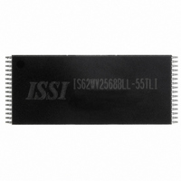
IS62WV2568BLL-55TLI ISSI, Integrated Silicon Solution Inc, IS62WV2568BLL-55TLI Datasheet - Page 8

IS62WV2568BLL-55TLI
Manufacturer Part Number
IS62WV2568BLL-55TLI
Description
IC SRAM 2MBIT 55NS 32TSOP
Manufacturer
ISSI, Integrated Silicon Solution Inc
Type
Asynchronousr
Datasheet
1.IS62WV2568BLL-55TLI.pdf
(14 pages)
Specifications of IS62WV2568BLL-55TLI
Memory Size
2M (256K x 8)
Package / Case
32-TSOP
Interface
Parallel
Format - Memory
RAM
Memory Type
SRAM - Asynchronous
Speed
55ns
Voltage - Supply
2.5 V ~ 3.6 V
Operating Temperature
-40°C ~ 85°C
Access Time
55 ns
Supply Voltage (max)
3.6 V
Supply Voltage (min)
2.5 V
Maximum Operating Current
15 mA
Organization
256 K x 8
Maximum Operating Temperature
+ 85 C
Minimum Operating Temperature
- 40 C
Mounting Style
SMD/SMT
Number Of Ports
1
Operating Supply Voltage
2.5 V to 3.6 V
Lead Free Status / RoHS Status
Lead free / RoHS Compliant
Lead Free Status / RoHS Status
Lead free / RoHS Compliant, Lead free / RoHS Compliant
Other names
706-1112
IS62WV2568BLL-55TLI
IS62WV2568BLL-55TLI
Available stocks
Company
Part Number
Manufacturer
Quantity
Price
Company:
Part Number:
IS62WV2568BLL-55TLI
Manufacturer:
ISSI
Quantity:
5 530
Company:
Part Number:
IS62WV2568BLL-55TLI
Manufacturer:
ISSI
Quantity:
2 148
Part Number:
IS62WV2568BLL-55TLI
Manufacturer:
ISSI
Quantity:
20 000
IS62WV2568ALL, IS62WV2568BLL
8
WRITE CYCLE SWITCHING CHARACTERISTICS
Notes:
1. Test conditions assume signal transition times of 5 ns or less, timing reference levels of 0.9V, input pulse levels of 0.4V to 1.4V
2. The internal write time is defined by the overlap of CS1 LOW, CS2 HIGH and WE LOW. All signals must be in valid states to
3. Tested with the load in Figure 2. Transition is measured ±500 mV from steady-state voltage. Not 100% tested.
AC WAVEFORMS
WRITE CYCLE NO. 1 (CS1/CS2 Controlled, OE = HIGH or LOW)
Symbol
t
t
t
t
t
t
t
t
t
t
Wc
scs
AW
hA
sA
PWe
sd
hd
hzWe
LzWe
ADDRESS
and output loading specified in Figure 1.
initiate a Write, but any one can go inactive to terminate the Write. The Data Input Setup and Hold timing are referenced to the
rising or falling edge of the signal that terminates the write.
1
/tscs
DOUT
CS1
CS2
2
DIN
WE
Parameter
Write Cycle Time
CS1/CS2 to Write End
Address Setup Time to Write End
Address Hold from Write End
Addrress Setup Time
WE Pulse Width
Data Setup to Write End
Data Hold from Write End
WE LOW to High-Z Output
WE HIGH to Low-Z Output
t
DATA UNDEFINED
SA
t
AW
t
HZWE
t
t
Min.
SCS2
SCS1
45
35
35
35
20
—
0
0
0
5
t
WC
t
45ns
PWE
(1,2)
HIGH-Z
Max.
20
—
—
—
—
—
—
—
—
—
(Over Operating Range)
Integrated Silicon Solution, Inc. — www.issi.com
t
SD
DATA-IN VALID
Min.
55
45
45
40
25
—
0
0
0
5
55ns
Max.
t
HA
20
—
—
—
—
—
—
—
—
—
t
t
LZWE
HD
Min.
70
60
60
50
30
—
0
0
0
5
70ns
Max
—
—
—
—
—
—
—
—
20
—
Unit
ns
ns
ns
ns
ns
ns
ns
ns
ns
ns
Rev. H
1/6/10


