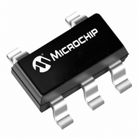
24LC02BT-I/OT Microchip Technology, 24LC02BT-I/OT Datasheet - Page 7

24LC02BT-I/OT
Manufacturer Part Number
24LC02BT-I/OT
Description
IC EEPROM 2KBIT 400KHZ SOT23-5
Manufacturer
Microchip Technology
Specifications of 24LC02BT-I/OT
Memory Size
2K (256 x 8)
Package / Case
SOT-23-5, SC-74A, SOT-25
Operating Temperature
-40°C ~ 85°C
Format - Memory
EEPROMs - Serial
Memory Type
EEPROM
Speed
400kHz
Interface
I²C, 2-Wire Serial
Voltage - Supply
2.5 V ~ 5.5 V
Organization
256 K x 8
Interface Type
I2C
Maximum Clock Frequency
0.4 MHz
Access Time
900 ns
Supply Voltage (max)
5.5 V
Supply Voltage (min)
2.5 V
Maximum Operating Current
3 mA
Maximum Operating Temperature
+ 85 C
Mounting Style
SMD/SMT
Minimum Operating Temperature
- 40 C
Operating Supply Voltage
2.5 V, 5.5 V
Lead Free Status / RoHS Status
Lead free / RoHS Compliant
Lead Free Status / RoHS Status
Lead free / RoHS Compliant, Lead free / RoHS Compliant
Other names
24LC02BT-I/OT
24LC02BTI/OT
24LC02BTI/OT
Available stocks
Company
Part Number
Manufacturer
Quantity
Price
Company:
Part Number:
24LC02BT-I/OT
Manufacturer:
MICROCHIP
Quantity:
12 000
Part Number:
24LC02BT-I/OT
Manufacturer:
MICROCHIP/微芯
Quantity:
20 000
5.0
A control byte is the first byte received following the
Start condition from the master device. The control byte
consists of a four-bit control code. For the 24XX02, this
is set as ‘
The next three bits of the control byte are “don’t cares”
for the 24XX02.
The last bit of the control byte defines the operation to
be performed. When set to ‘
selected. When set to ‘
Following the Start condition, the 24XX02 monitors the
SDA bus, checking the device type identifier being
transmitted and, upon a
outputs an Acknowledge signal on the SDA line.
Depending on the state of the R/W bit, the 24XX02 will
select a read or write operation.
FIGURE 5-2:
© 2009 Microchip Technology Inc.
Operation
Read
Write
DEVICE ADDRESSING
1010’
Control
x = “don’t care”
binary for read and write operations.
1010
1010
Code
1
Control
Code
0
0
ADDRESS SEQUENCE BIT ASSIGNMENTS
’, a write operation is selected.
‘1010’
1
Control Byte
Block Address
Block Address
Block Select
0
1
’, a read operation is
code, the slave device
x
Select
Block
bits
x
x
R/W
R/W
1
0
FIGURE 5-1:
A
7
Start Bit
x = “don’t care”
•
S
Address Low Byte
24AA02/24LC02B
•
1
Control Code
•
0
•
Slave Address
1
•
CONTROL BYTE
ALLOCATION
0
•
A
0
x
Select
Block
Bits
x
Acknowledge Bit
Read/Write Bit
x
DS21709J-page 7
R/W ACK


