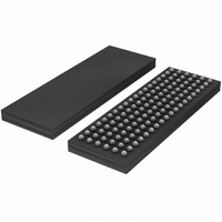
74ALVCH32501EC,551 NXP Semiconductors, 74ALVCH32501EC,551 Datasheet - Page 2

74ALVCH32501EC,551
Manufacturer Part Number
74ALVCH32501EC,551
Description
IC UNIV BUS TXRX 26BIT 114LFBGA
Manufacturer
NXP Semiconductors
Series
74ALVCHr
Datasheet
1.74ALVCH32501EC518.pdf
(15 pages)
Specifications of 74ALVCH32501EC,551
Logic Type
Universal Bus Transceiver
Number Of Circuits
36-Bit
Current - Output High, Low
24mA, 24mA
Voltage - Supply
2.3 V ~ 3.6 V
Operating Temperature
-40°C ~ 85°C
Mounting Type
Surface Mount
Package / Case
114-LFBGA
Lead Free Status / RoHS Status
Lead free / RoHS Compliant
Other names
74ALVCH32501EC-S
74ALVCH32501EC-S
935266783551
74ALVCH32501EC-S
935266783551
Available stocks
Company
Part Number
Manufacturer
Quantity
Price
Company:
Part Number:
74ALVCH32501EC,551
Manufacturer:
NXP Semiconductors
Quantity:
10 000
Philips Semiconductors
FEATURES
DESCRIPTION
The 74ALVCH32501 is a high-performance CMOS
product designed for V
Active bus-hold circuitry is provided to hold unused or
floating data inputs at a valid logic level.
QUICK REFERENCE DATA
GND = 0 V; T
Note
1. C
2004 Oct 13
t
C
C
C
PHL
SYMBOL
3-state non-inverting outputs for bus oriented
applications
Wide supply voltage range of 1.2 V to 3.6 V
Complies with JEDEC standard no. 8-1A
Current drive 24 mA at 3.0 V
Universal bus transceiver with D-type latches and
D-type flip-flops capable of operating in transparent,
latched or clocked mode
CMOS low power consumption
Direct interface with TTL levels
All inputs have bus-hold circuitry
Output drive capability 50
Plastic fine-pitch ball grid array package.
I
I/O
PD
36-bit universal bus transceiver with direction pin;
3-state
P
f
f
C
V
N = number of inputs switching;
i
o
/t
(C
D
CC
PD
= input frequency in MHz;
L
PLH
= output frequency in MHz;
= output load capacitance in pF;
= C
L
is used to determine the dynamic power dissipation (P
= supply voltage in Volts;
PD
V
CC
amb
propagation delay A
input capacitance
input/output capacitance
power dissipation capacitance per latch
2
V
CC
= 25 C; t
f
o
2
) = sum of the outputs.
CC
f
i
operation at 2.5 V and 3.3 V.
N + (C
r
PARAMETER
= t
f
transmission lines at 85 C
2.5 ns.
n
L
to B
V
CC
n
; B
2
n
to A
f
o
) where:
n
C
C
V
I
L
L
2
outputs enabled
outputs disabled
= GND to V
= 30 pF; V
= 50 pF; V
The 74ALVCH32501 can be used as two 18-bit
transceivers or one 36-bit transceiver featuring
non-inverting 3-state bus compatible outputs in both send
and receive directions. Data flow in each direction is
controlled by output enable (OE
(LE
For A-to-B data flow, the device operates in the
transparent mode when LE
LOW, the A data is latched if input CP
or LOW level. If input LE
the latch/flip-flop on the LOW-to-HIGH transition of CP
When input OE
input OE
state.
Data flow for B-to-A is similar to that of A-to-B, but uses
inputs OE
complimentary (OE
LOW).
To ensure the high-impedance state during power-up or
power-down, pin OE
pull-up resistor and pin OE
through a pull-down resistor. The minimum value of the
resistor is determined by the current-sinking or
current-sourcing capability of the driver.
D
AB
in W).
and LE
CONDITIONS
AB
CC
CC
BA
CC
is LOW, the outputs are in the high-impedance
, LE
= 2.5 V
= 3.3 V
; note 1
BA
AB
), and clock inputs (CP
BA
is HIGH, the outputs are active. When
and CP
AB
BA
is active HIGH, and OE
should be tied to V
AB
AB
BA
AB
is LOW, the A data is stored in
. The output enables are
is HIGH. When input LE
should be tied to GND
AB
74ALVCH32501
and OE
Product specification
2.8
3.0
4.0
8.0
21
3
AB
TYP.
AB
is held at a HIGH
BA
and CP
CC
), latch enable
through a
BA
ns
ns
pF
pF
pF
pF
is active
BA
UNIT
).
AB
AB
is
.


