74ALVCH16501DL,112 NXP Semiconductors, 74ALVCH16501DL,112 Datasheet - Page 5
74ALVCH16501DL,112
Manufacturer Part Number
74ALVCH16501DL,112
Description
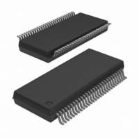
IC 18BIT UNVRSL BUS TXRX 56-SSOP
Manufacturer
NXP Semiconductors
Series
74ALVCHr
Datasheet
1.74ALVCH16501DL112.pdf
(18 pages)
Specifications of 74ALVCH16501DL,112
Logic Type
Universal Bus Transceiver
Number Of Circuits
18-Bit
Current - Output High, Low
24mA, 24mA
Voltage - Supply
2.3 V ~ 2.7 V
Operating Temperature
-40°C ~ 85°C
Mounting Type
Surface Mount
Package / Case
56-SSOP
Lead Free Status / RoHS Status
Lead free / RoHS Compliant
Other names
74ALVCH16501DL
74ALVCH16501DL
935263882112
74ALVCH16501DL
935263882112


NXP Semiconductors
Table 2.
6. Functional description
Table 3.
[1]
7. Limiting values
Table 4.
In accordance with the Absolute Maximum Rating System (IEC 60134). Voltages are referenced to GND (ground = 0 V).
74ALVCH16501_3
Product data sheet
Symbol
CPBA
B0 to B17
CPAB
Inputs
OEAB
L
H
H
H
H
H
H
H
H
Symbol
V
I
V
I
V
I
I
IK
OK
O
CC
CC
I
O
A-to-B data flow is shown; B-to-A flow is similar but uses OEBA, LEBA and CPBA.
H = HIGH voltage level;
h = HIGH voltage level one set-up time prior to the enable or clock transition;
L = LOW voltage level;
l = LOW voltage level one set-up time prior to the enable or clock transition;
X = don’t care;
Z = high-impedance OFF-state;
↓
↑ = LOW-to-HIGH clock transition.
= HIGH-to-LOW clock transition;
Pin description
Function table
Limiting values
Parameter
supply voltage
input clamping current
input voltage
output clamping current
output voltage
output current
supply current
LEAB
X
H
H
↓
↓
L
L
L
L
6.1 Function table
Pin
30
54, 52, 51, 49, 48, 47, 45, 44, 43, 42, 41, 40, 38, 37, 36, 34, 33, 31
55
[1]
…continued
CPAB
X
X
X
X
X
↑
↑
H or L
H or L
Conditions
V
control inputs
data inputs
V
V
All information provided in this document is subject to legal disclaimers.
I
O
O
< 0 V
> V
= 0 V to V
An
X
H
L
h
l
h
l
X
X
CC
Rev. 03 — 2 April 2010
or V
CC
O
< 0 V
Output
Bn
Z
H
L
H
L
H
L
H
L
18-bit universal bus transceiver; 3-state
Operating mode
disabled
transparent
latch data and display
clock data and display
hold data and display
[1]
[1]
[1]
74ALVCH16501
Description
clock input B-to-A
data inputs or outputs
clock input A-to-B
Min
−0.5
−50
−0.5
−0.5
-
−0.5
-
-
Max
+4.6
-
+4.6
V
±50
V
±50
100
CC
CC
© NXP B.V. 2010. All rights reserved.
+ 0.5
+ 0.5
Unit
V
mA
V
V
mA
V
mA
mA
5 of 18
Related parts for 74ALVCH16501DL,112
Image
Part Number
Description
Manufacturer
Datasheet
Request
R

Part Number:
Description:
NXP Semiconductors designed the LPC2420/2460 microcontroller around a 16-bit/32-bitARM7TDMI-S CPU core with real-time debug interfaces that include both JTAG andembedded trace
Manufacturer:
NXP Semiconductors
Datasheet:

Part Number:
Description:
NXP Semiconductors designed the LPC2458 microcontroller around a 16-bit/32-bitARM7TDMI-S CPU core with real-time debug interfaces that include both JTAG andembedded trace
Manufacturer:
NXP Semiconductors
Datasheet:
Part Number:
Description:
NXP Semiconductors designed the LPC2468 microcontroller around a 16-bit/32-bitARM7TDMI-S CPU core with real-time debug interfaces that include both JTAG andembedded trace
Manufacturer:
NXP Semiconductors
Datasheet:
Part Number:
Description:
NXP Semiconductors designed the LPC2470 microcontroller, powered by theARM7TDMI-S core, to be a highly integrated microcontroller for a wide range ofapplications that require advanced communications and high quality graphic displays
Manufacturer:
NXP Semiconductors
Datasheet:
Part Number:
Description:
NXP Semiconductors designed the LPC2478 microcontroller, powered by theARM7TDMI-S core, to be a highly integrated microcontroller for a wide range ofapplications that require advanced communications and high quality graphic displays
Manufacturer:
NXP Semiconductors
Datasheet:
Part Number:
Description:
The Philips Semiconductors XA (eXtended Architecture) family of 16-bit single-chip microcontrollers is powerful enough to easily handle the requirements of high performance embedded applications, yet inexpensive enough to compete in the market for hi
Manufacturer:
NXP Semiconductors
Datasheet:
Part Number:
Description:
The XA-S3 device is a member of Philips Semiconductors? XA(eXtended Architecture) family of high performance 16-bitsingle-chip microcontrollers
Manufacturer:
NXP Semiconductors
Datasheet:

Part Number:
Description:
The NXP BlueStreak LH75401/LH75411 family consists of two low-cost 16/32-bit System-on-Chip (SoC) devices
Manufacturer:
NXP Semiconductors
Datasheet:
Part Number:
Description:
The NXP LPC3130/3131 combine an 180 MHz ARM926EJ-S CPU core, high-speed USB2
Manufacturer:
NXP Semiconductors
Datasheet:
Part Number:
Description:
The NXP LPC3141 combine a 270 MHz ARM926EJ-S CPU core, High-speed USB 2
Manufacturer:
NXP Semiconductors
Part Number:
Description:
The NXP LPC3143 combine a 270 MHz ARM926EJ-S CPU core, High-speed USB 2
Manufacturer:
NXP Semiconductors

Part Number:
Description:
The NXP LPC3152 combines an 180 MHz ARM926EJ-S CPU core, High-speed USB 2
Manufacturer:
NXP Semiconductors
Part Number:
Description:
The NXP LPC3154 combines an 180 MHz ARM926EJ-S CPU core, High-speed USB 2
Manufacturer:
NXP Semiconductors

Part Number:
Description:
Standard level N-channel enhancement mode Field-Effect Transistor (FET) in a plastic package using NXP High-Performance Automotive (HPA) TrenchMOS technology
Manufacturer:
NXP Semiconductors
Datasheet: