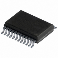
74LVC4245ADB,118 NXP Semiconductors, 74LVC4245ADB,118 Datasheet - Page 7

74LVC4245ADB,118
Manufacturer Part Number
74LVC4245ADB,118
Description
IC TRANSCVR TRI-ST DL 24SSOP
Manufacturer
NXP Semiconductors
Series
74LVCr
Datasheet
1.74LVC4245APW112.pdf
(17 pages)
Specifications of 74LVC4245ADB,118
Output Type
TTL
Package / Case
24-SSOP
Logic Function
Translator, 3-State
Number Of Bits
8
Input Type
TTL
Number Of Channels
8
Number Of Outputs/channel
1
Differential - Input:output
No/No
Propagation Delay (max)
8ns
Voltage - Supply
1.5 V ~ 5.5 V
Operating Temperature
-40°C ~ 125°C
Supply Voltage
1.5 V ~ 5.5 V
Logic Family
LVC
Number Of Channels Per Chip
8
Input Level
LVTTL
Output Level
LVTTL
High Level Output Current
- 24 mA
Low Level Output Current
24 mA
Propagation Delay Time
3.6 ns
Supply Voltage (max)
3.6 V, 5.5 V
Supply Voltage (min)
1.5 V
Maximum Operating Temperature
+ 125 C
Function
Bus Transceiver with Voltage Translation
Input Bias Current (max)
40 uA
Minimum Operating Temperature
- 40 C
Mounting Style
SMD/SMT
Polarity
Non-Inverting
Logic Type
CMOS
Number Of Circuits
1
Dc
1105
Lead Free Status / RoHS Status
Lead free / RoHS Compliant
Data Rate
-
Lead Free Status / Rohs Status
Lead free / RoHS Compliant
Other names
74LVC4245ADB-T
74LVC4245ADB-T
935260750118
74LVC4245ADB-T
935260750118
NXP Semiconductors
Table 6.
At recommended operating conditions; voltages are referenced to GND (ground = 0 V).
[1]
[2]
[3]
10. Dynamic characteristics
Table 7.
Voltages are referenced to GND (ground = 0 V). V
74LVC4245A_6
Product data sheet
Symbol
Symbol Parameter
t
t
t
t
t
t
PHL
PLH
PZL
PZH
PLZ
PHZ
I
CC
All typical values are measured at V
For transceivers, the parameter I
V
V
CCB
CCA
= 2.7 V to 3.6 V: other inputs at V
= 4.5 V to 5.5 V: other inputs at V
HIGH to LOW
propagation
delay
LOW to HIGH
propagation
delay
OFF-state to
LOW
propagation
delay
OFF-state to
HIGH
propagation
delay
LOW to
OFF-state
propagation
delay
HIGH to
OFF-state
propagation
delay
Parameter
additional supply current
Static characteristics
Dynamic characteristics
Conditions
An to Bn;
see
Bn to An;
see
An to Bn;
see
Bn to An;
see
OE to An;
see
OE to Bn;
see
OE to An;
see
OE to Bn;
see
OE to An;
see
OE to Bn;
see
OE to An;
see
OE to Bn;
see
Figure 6
Figure 6
Figure 6
Figure 6
Figure 7
Figure 7
Figure 7
Figure 7
Figure 7
Figure 7
Figure 7
Figure 7
OZ
…continued
includes the input leakage current.
CCA
CCB
CCA
Conditions
per control pin; I
= 5.0 V, V
V
V
other inputs at V
V
V
other inputs at V
CCB
I
CCA
I
or GND.
or GND.
= V
= V
= 2.7 V to 3.6 V;
= 4.5 V to 5.5 V;
CCB
CCA
CCB
V
2.7 V
3.0 V to 3.6 V
2.7 V
3.0 V to 3.6 V
2.7 V
3.0 V to 3.6 V
2.7 V
3.0 V to 3.6 V
2.7 V
3.0 V to 3.6 V
2.7 V
3.0 V to 3.6 V
2.7 V
3.0 V to 3.6 V
2.7 V
3.0 V to 3.6 V
2.7 V
3.0 V to 3.6 V
2.7 V
3.0 V to 3.6 V
2.7 V
3.0 V to 3.6 V
2.7 V
3.0 V to 3.6 V
Rev. 06 — 18 January 2008
CCA
CCB
= 3.3 V and T
0.6 V;
0.6 V;
= 4.5 V to 5.5 V; t
O
= 0 A
CCB
CCA
or GND
or GND
amb
Octal dual supply translating transceiver; 3-state
= 25 C.
1.0
1.0
1.0
1.0
1.0
1.0
1.0
1.0
1.0
1.0
1.0
1.0
1.0
1.0
1.0
1.0
1.0
1.0
1.0
1.0
1.0
1.0
1.0
1.0
r
Min
= t
40 C to +85 C
f
2.5 ns. For test circuit see
3.6
3.3
3.4
3.4
3.3
2.8
3.0
3.0
4.5
4.5
4.4
3.8
4.5
4.5
4.3
3.2
2.9
2.9
3.9
3.5
2.8
2.8
3.3
2.9
Typ
[3]
[1]
Min
-
-
6.3
6.3
6.1
6.1
6.7
6.5
5.0
5.0
9.0
9.0
8.7
8.1
8.1
8.1
8.7
8.1
7.0
7.0
7.7
7.7
5.8
5.8
7.8
7.8
Max
74LVC4245A
1.0
1.0
1.0
1.0
1.0
1.0
1.0
1.0
1.0
1.0
1.0
1.0
1.0
1.0
1.0
1.0
1.0
1.0
1.0
1.0
1.0
1.0
1.0
1.0
40 C to +125 C Unit
Min
Typ
-
-
© NXP B.V. 2008. All rights reserved.
[1]
Figure
8.0
8.0
8.0
8.0
8.5
8.5
6.5
6.5
11.5
11.5
11.0
10.5
10.5
10.5
11.0
10.5
9.0
9.0
10.0
10.0
7.5
7.5
10.0
10.0
Max
5000
5000
Max
8.
Unit
ns
ns
ns
ns
ns
ns
ns
ns
ns
ns
ns
ns
ns
ns
ns
ns
ns
ns
ns
ns
ns
ns
ns
ns
A
A
7 of 17


