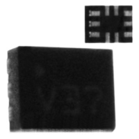
ST2129QTR STMicroelectronics, ST2129QTR Datasheet

ST2129QTR
Specifications of ST2129QTR
Available stocks
Related parts for ST2129QTR
ST2129QTR Summary of contents
Page 1
... QFN10 (1.8 x 1.4 mm) Applications ■ Low voltage system level translation ■ Mobile phones and other mobile devices Table 1. Device summary Order Code ST2129QTR September 2009 2-bit dual supply level translator without direction control pin ): L supply CC Description The ST2129 is a 2-bit dual supply level translator which provides the level shifting capability to allow data transfer in a multi-voltage system ...
Page 2
Pin settings 1 Pin settings 1.1 Pin connection Figure 1. Pin connection (top through view) I/O VL1 I/O 1.2 Pin description Table 2. Pin description Pin number 2/ ...
Page 3
ST2129 2 Logic diagram Figure 2. Logic block diagram 2.1 Device block diagrams Figure 3. ST2129 block diagram Doc ID 15967 Rev 1 Logic diagram 3/20 ...
Page 4
Logic diagram Figure 4. Application block diagram V L 0 system controller I/O I/O VL1 I/O I/O VL2 OE Doc ID 15967 Rev 1 0 system controller VCC1 VCC2 ...
Page 5
ST2129 3 Supplementary notes 3.1 Driver requirement For proper operation, the driver from each side of the device must have the capability to source and sink a minimum of 1mA current. The device architecture requires the driver to source/sink a ...
Page 6
Maximum ratings 4 Maximum ratings Stressing the device above the rating listed in device. These are stress ratings only and operation of the device at these or any other conditions above those indicated in the operating sections of this specification ...
Page 7
ST2129 5 Electrical characteristics Over recommended operating conditions unless otherwise noted. All typical values are °C. A Table 6. DC characteristics Symbol Parameter V L 1.65 1.8 High level input V 2.5 IHL voltage (I/O ) ...
Page 8
Electrical characteristics Table 6. DC characteristics (continued) Symbol Parameter V L 1.65 1.8 High level input V 2.5 IH-OE voltage (OE) 3.0 3.6 1.65 1.8 Low level input V 2.5 IL-OE voltage (OE) 3.0 3.6 High level 1. ...
Page 9
ST2129 DC characteristics Table 7. Symbol Parameter V Control input 1. leakage OE 3.6 current (OE) High impedance 1. leakage IO_LKG 3.6 current (I I/O ) VCC Partial power 1. OFF down ...
Page 10
AC characteristics 6 AC characteristics Load pF; driver t L Table 8. AC characteristics - test conditions: V Symbol Parameter t Rise time I/O RVCC VCC t Fall time I/O FVCC VCC t Rise time I/O RVL ...
Page 11
ST2129 Table 9. AC characteristics - test conditions: V Symbol Parameter t Rise time I/O RVCC VCC t Fall time I/O FVCC VCC t Rise time I/O RVL VL t Fall time I/O FVL VL Propagation delay time I/O to ...
Page 12
AC characteristics Table 10. AC characteristics - test conditions: V Symbol Parameter t t Output enable time PZL PZH t t Output disable time PLZ PHZ (1) D Data rate R 1. Data rate is guaranteed based on the condition ...
Page 13
ST2129 7 Test circuit Figure 5. Test circuit Pulse generator Table 11. Test circuit switches Test t t PLH, PHL PZL, PLZ t t PZH, PHZ Table 12. Waveform symbol value Symbol V ...
Page 14
Test circuit Figure 6. Waveform - propagation delay ( MHz, 50% duty cycle) Figure 7. Waveform - output enable and disable time ( MHz, 50% duty cycle) 14/20 Doc ID 15967 Rev 1 ST2129 ...
Page 15
ST2129 8 Package mechanical data In order to meet environmental requirements, ST offers these devices in different grades of ® ECOPACK packages, depending on their level of environmental compliance. ECOPACK specifications, grade definitions and product status are available at: www.st.com. ...
Page 16
Package mechanical data Table 13. Mechanical data for QFN10 (1.8 x 1.4 x 0.5 mm) - 0.40 mm pitch Symbol Figure 9. Footprint recommendation for QFN10 (1.8 x 1.4 x 0.5 mm) ...
Page 17
ST2129 Figure 10. Carrier tape for QFN10 (1.8 x 1.4 x 0.5 mm) - 0.40 mm pitch Figure 11. Reel information for QFN10 (1.8 x 1.4 x 0.5 mm) - 0.40 mm pitch Doc ID 15967 Rev 1 Package mechanical ...
Page 18
Package mechanical data Figure 12. Reel information for QFN10 (1.8 x 1.4 x 0.5 mm) - 0.40 mm pitch 18/20 Doc ID 15967 Rev 1 ST2129 ...
Page 19
ST2129 9 Revision history Table 14. Document revision history Date 07-Sep-2009 Revision 1 Initial release. Doc ID 15967 Rev 1 Revision history Changes 19/20 ...
Page 20
... Information in this document is provided solely in connection with ST products. STMicroelectronics NV and its subsidiaries (“ST”) reserve the right to make changes, corrections, modifications or improvements, to this document, and the products and services described herein at any time, without notice. All ST products are sold pursuant to ST’s terms and conditions of sale. ...


