74AUP1T58GW,125 NXP Semiconductors, 74AUP1T58GW,125 Datasheet
74AUP1T58GW,125
Specifications of 74AUP1T58GW,125
74AUP1T58GW,125
74AUP1T58GW-G
74AUP1T58GW-G
935280466125


Related parts for 74AUP1T58GW,125


74AUP1T58GW,125 Summary of contents
Page 1
Low-power configurable gate with voltage-level translator Rev. 01 — 6 March 2008 1. General description The 74AUP1T58 provides low-power, low-voltage configurable logic gate functions. The output state is determined by eight patterns of 3-bit input. The user can choose ...
Page 2
... NXP Semiconductors 3. Ordering information Table 1. Ordering information Type number Package Temperature range Name 74AUP1T58GW +125 C 74AUP1T58GM +125 C 74AUP1T58GF +125 C 4. Marking Table 2. Marking Type number 74AUP1T58GW 74AUP1T58GM 74AUP1T58GF 5. Functional diagram Fig 1. Logic symbol 74AUP1T58_1 Product data sheet Low-power configurable gate with voltage-level translator ...
Page 3
... NXP Semiconductors 6. Pinning information 6.1 Pinning 74AUP1T58 GND 001aah836 Fig 2. Pin configuration SOT363 (SC-88) 6.2 Pin description Table 3. Pin description Symbol Pin B 1 GND Functional description [1] Table 4. Function table Input [ HIGH voltage level LOW voltage level. 74AUP1T58_1 Product data sheet Low-power confi ...
Page 4
... NXP Semiconductors 7.1 Logic configurations Table 5. Function selection table Logic function 2-input NAND 2-input NAND with both inputs inverted 2-input AND with inverted input 2-input NOR with inverted input 2-input OR 2-input OR with both inputs inverted 2-input XOR Buffer Inverter Fig 5. ...
Page 5
... NXP Semiconductors Fig 11. Inverter 8. Limiting values Table 6. Limiting values In accordance with the Absolute Maximum Rating System (IEC 60134). Voltages are referenced to GND (ground = 0 V). Symbol Parameter V supply voltage CC I input clamping current IK V input voltage I I output clamping current OK V output voltage ...
Page 6
... NXP Semiconductors 10. Static characteristics Table 8. Static characteristics At recommended operating conditions; voltages are referenced to GND (ground = 0 V). Symbol Parameter amb V positive-going threshold T+ voltage V negative-going threshold T voltage V hysteresis voltage H V HIGH-level output voltage OH V LOW-level output voltage OL I input leakage current I I power-off leakage current ...
Page 7
... NXP Semiconductors Table 8. Static characteristics At recommended operating conditions; voltages are referenced to GND (ground = 0 V). Symbol Parameter V HIGH-level output voltage OH V LOW-level output voltage OL I input leakage current I I power-off leakage current OFF I additional power-off OFF leakage current I supply current CC I additional supply current ...
Page 8
... NXP Semiconductors Table 8. Static characteristics At recommended operating conditions; voltages are referenced to GND (ground = 0 V). Symbol Parameter I power-off leakage current OFF I additional power-off OFF leakage current I supply current CC I additional supply current CC [1] One input at 0 1.1 V, other input at V [2] One input at 0. 1.2 V, other input ...
Page 9
... NXP Semiconductors Table 9. Dynamic characteristics Voltages are referenced to GND (ground = 0 V); for test circuit see Symbol Parameter Conditions propagation delay see propagation delay see amb C power dissipation MHz capacitance V V [1] All typical values are measured at nominal V [2] ...
Page 10
... NXP Semiconductors 12. Waveforms input Measurement points are given in V and V are typical output voltage levels that occur with the output load Fig 12. Input A, B and C to output Y propagation delay times Table 10. Measurement points Supply voltage Output 2 3.6 V 0.5 74AUP1T58_1 Product data sheet Low-power confi ...
Page 11
... NXP Semiconductors Test data is given in Table Definitions for test circuit Load resistance Load capacitance including jig and probe capacitance Termination resistance should be equal to the output impedance External voltage for measuring switching times. EXT Fig 13. Load circuitry for switching times Table 11. ...
Page 12
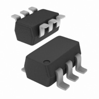
... NXP Semiconductors 13. Package outline Plastic surface-mounted package; 6 leads y 6 pin 1 index DIMENSIONS (mm are the original dimensions UNIT max 0.30 1.1 0.25 mm 0.1 0.20 0.8 0.10 OUTLINE VERSION IEC SOT363 Fig 14. Package outline SOT363 (SC-88) 74AUP1T58_1 Product data sheet Low-power configurable gate with voltage-level translator ...
Page 13
... NXP Semiconductors XSON6: plastic extremely thin small outline package; no leads; 6 terminals; body 1 x 1. (2) terminal 1 index area DIMENSIONS (mm are the original dimensions) ( UNIT b D max max 0.25 1.5 mm 0.5 0.04 0.17 1.4 Notes 1. Including plating thickness. 2. Can be visible in some manufacturing processes. ...
Page 14
... NXP Semiconductors XSON6: plastic extremely thin small outline package; no leads; 6 terminals; body 0 (1) terminal 1 index area DIMENSIONS (mm are the original dimensions UNIT b D max max 0.20 1.05 mm 0.5 0.04 0.12 0.95 Note 1. Can be visible in some manufacturing processes. OUTLINE VERSION IEC SOT891 Fig 16 ...
Page 15
... NXP Semiconductors 14. Abbreviations Table 12. Abbreviations Acronym Description CDM Charged Device Model CMOS Complementary Metal Oxide Semiconductor DUT Device Under Test ESD ElectroStatic Discharge HBM Human Body Model MM Machine Model TTL Transistor-Transistor Logic 15. Revision history Table 13. Revision history Document ID Release date 74AUP1T58_1 ...
Page 16
... Right to make changes — NXP Semiconductors reserves the right to make changes to information published in this document, including without limitation specifications and product descriptions, at any time and without notice ...
Page 17
... NXP Semiconductors 18. Contents 1 General description . . . . . . . . . . . . . . . . . . . . . . 1 2 Features . . . . . . . . . . . . . . . . . . . . . . . . . . . . . . . 1 3 Ordering information . . . . . . . . . . . . . . . . . . . . . 2 4 Marking . . . . . . . . . . . . . . . . . . . . . . . . . . . . . . . . 2 5 Functional diagram . . . . . . . . . . . . . . . . . . . . . . 2 6 Pinning information . . . . . . . . . . . . . . . . . . . . . . 3 6.1 Pinning . . . . . . . . . . . . . . . . . . . . . . . . . . . . . . . 3 6.2 Pin description . . . . . . . . . . . . . . . . . . . . . . . . . 3 7 Functional description . . . . . . . . . . . . . . . . . . . 3 7.1 Logic configurations . . . . . . . . . . . . . . . . . . . . . 4 8 Limiting values Recommended operating conditions Static characteristics Dynamic characteristics . . . . . . . . . . . . . . . . . . 8 12 Waveforms ...