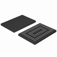
SSTUH32865ET,518 NXP Semiconductors, SSTUH32865ET,518 Datasheet - Page 15

SSTUH32865ET,518
Manufacturer Part Number
SSTUH32865ET,518
Description
IC BUFFER 1.8V 28BIT SOT802
Manufacturer
NXP Semiconductors
Datasheet
1.SSTUH32865ETG551.pdf
(28 pages)
Specifications of SSTUH32865ET,518
Logic Type
1:2 Registered Buffer with Parity
Supply Voltage
1.7 V ~ 1.9 V
Number Of Bits
28
Operating Temperature
0°C ~ 70°C
Mounting Type
Surface Mount
Package / Case
160-TFBGA
Lead Free Status / RoHS Status
Lead free / RoHS Compliant
Other names
935277962518
SSTUH32865ET-T
SSTUH32865ET-T
SSTUH32865ET-T
SSTUH32865ET-T
Philips Semiconductors
8. Limiting values
Table 6:
In accordance with the Absolute Maximum Rating System (IEC 60134).
[1]
[2]
9. Recommended operating conditions
Table 7:
[1]
[2]
9397 750 14136
Product data sheet
Symbol
V
V
V
I
I
I
I
T
V
Symbol
V
V
V
V
V
V
V
V
V
V
V
V
I
I
T
IK
OK
O
CCC
OH
OL
stg
amb
DD
I
O
esd
DD
REF
TT
I
IH(AC)
IL(AC)
IH(DC)
IL(DC)
IH
IL
ICR
ID
Stresses beyond those listed under ‘absolute maximum ratings’ may cause permanent damage to the device. These are stress ratings
only and functional operation of the device at these or any other conditions beyond those indicated under ‘recommended operating
conditions’ is not implied. Exposure to absolute-maximum-rated conditions for extended periods may affect device reliability.
The input and output negative-voltage ratings may be exceeded if the input and output current ratings are observed.
The differential inputs must not be floating, unless RESET is LOW.
The RESET input of the device must be held at valid logic levels (not floating) to ensure proper device operation.
Limiting values
Recommended operating conditions
Parameter
supply voltage
receiver input voltage
driver output voltage
input clamp current
output clamp current
continuous output current
continuous current through
each V
storage temperature
electrostatic discharge
voltage
Parameter
supply voltage
reference voltage
termination voltage
input voltage
AC HIGH-level input voltage
AC LOW-level input voltage
DC HIGH-level input voltage
DC LOW-level input voltage
HIGH-level input voltage
LOW-level input voltage
common mode input voltage
range
differential input voltage
HIGH-level output current
LOW-level output current
operating ambient temperature
in free air
DD
or GND pin
Conditions
V
V
0 V < V
Human Body Model (HBM); 1.5 k ;
100 pF
Machine Model (MM); 0 ; 200 pF
I
O
< 0 V or V
Conditions
data inputs (Dn)
data inputs (Dn)
data inputs (Dn)
data inputs (Dn)
RESET
RESET
CK, CK
CK, CK
< 0 V or V
Rev. 01 — 11 March 2005
O
< V
I
DD
O
> V
1.8 V high output drive DDR registered buffer with parity
> V
DD
DD
[1]
[1]
[1]
[1]
[2]
[2]
Min
1.7
0.49
V
0
V
-
V
-
0.65
-
0.675
600
-
-
0
REF
REF
REF
+ 250 mV
+ 125 mV
V
V
40 mV
DD
DD
[2]
[2]
Typ
-
0.50
V
-
-
-
-
-
-
-
-
-
-
-
-
REF
Min
-
-
-
-
2
200
© Koninklijke Philips Electronics N.V. 2005. All rights reserved.
0.5
0.5
0.5
65
SSTUH32865
V
DD
Max
1.9
0.51
V
V
-
V
-
V
-
0.35
1.125
-
12
+70
Max
+2.5
+2.5
V
+150
-
-
12
REF
DD
REF
REF
50
50
50
100
DD
+ 40 mV
+ 0.5
V
V
250 mV
125 mV
DD
DD
Unit
V
V
V
mA
mA
mA
mA
kV
V
C
15 of 28
Unit
V
V
V
V
V
V
V
V
V
V
V
mV
mA
mA
C


