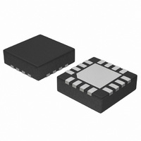
NB7VPQ16MMNG ON Semiconductor, NB7VPQ16MMNG Datasheet

NB7VPQ16MMNG
Specifications of NB7VPQ16MMNG
Available stocks
Related parts for NB7VPQ16MMNG
NB7VPQ16MMNG Summary of contents
Page 1
NB7VPQ16M 1.8V/2.5V CML 12.5 Gbps Programmable Pre-Emphasis Copper/Cable Driver with Selectable Equalizer Receiver Multi−Level Inputs w/ Internal Termination Description The NB7VPQ16M is a high performance single channel programmable Pre−Emphasis CML Driver with a selectable Equalizer Receiver that operates up to ...
Page 2
Multi−Level Inputs LVPECL, LVDS, CML (2) IN 50W (1) VT 50W (3) IN Figure 2. Detailed Block Diagram of NB7VPQ16M Q Low Q High Bit n − OD0dB V ODPE Figure 3. Illustration of Output Waveform ...
Page 3
Table 1. TYPICAL PRE−EMPHASIS CONTROL TABLE 255C, V MSB D3 Decimal ...
Page 4
Table 3. PIN DESCRIPTION Pin Name I LVPECL, CML, LVDS Input 3 IN LVPECL, CML, LVDS Input 4 GND − 5 VCCD − 6 SDOUT LVCMOS Output 7 SCLKOUT LVCMOS Output 8 GND − 9 VCC ...
Page 5
Table 4. ATTRIBUTES ESD Protection Internal Input Pulldown Resistor Moisture Sensitivity, Indefinite Time Out of Drypack (Note 3) Flammability Rating Transistor Count Meets or exceeds JEDEC Spec EIA/JESD78 IC Latchup Test 3. For additional information, see Application Note AND8003/D. Table ...
Page 6
Table 6. DC CHARACTERISTICS POSITIVE CML OUTPUT (Note 5) Symbol POWER SUPPLY CURRENT I Power Supply Current, (Inputs and Outputs Open 0dB I Power Supply Current for Serial Bus and DAC CCD (Inputs and Outputs Open) CML ...
Page 7
Table 7. AC CHARACTERISTICS V Symbol f Maximum Input Data Rate DATAMAX f Maximum Input Clock Frequency (Note 9) MAX f Serial Clock Input Frequency SCLKIN VOD Output Voltage Amplitude (see Table 1) 0dB (@ V ) (See Figure 3, ...
Page 8
IHD(IN IHD IN V ILD Figure 6. Differential Inputs Driven Differentially CMmax V CMR V CMmin GND SDIN SCLKIN Figure 9. SDIN/SCLKIN Setup and Hold Time IN ...
Page 9
Data Inputs The differential IN/IN inputs of the NB7VPQ16M can accept LVPECL, CML, and LVDS signal levels. The limitations for a differential input signal (LVDS, LVPECL, or CML minimum input swing of 100 mV (single−ended measurement). Within this ...
Page 10
SDOUT/SCLKOUT SDOUT is the Serial Data output pin; SCLKOUT is the Serial Clock output pin. These pins are the outputs of the 5−bit SDI shift register and will produce the SDIN/SCLKIN SDIN EQEN ...
Page 11
INA DUTA EQA SLOAD Serial Data In SDINA PEA Serial Clock In SCLKINA CML QA Figure 13. Simplified Cascaded Logic Diagram DUTC SDIN D3C D2C D1C D0C D3B EQC SCLKIN Clocks t PD SCLKIN ...
Page 12
Signal Generator Signal Generator Output 20 mV/div 28 ps/div Signal Generator Output 20 mV/div 28 ps/div Figure 15. Typical NB7VPQ16M Equalizer Application and Interconnect; Eye Diagrams with PRBS23 Pattern at NB7VPQ16M Equalizer Receiver and 1 FR4 = ...
Page 13
NB7VPQ16M Pre−emphasis Driver Q Signal Generator Q Signal Generator Output 20 mV/div 28 ps/div Signal Generator Output 20 mV/div 28 ps/div Figure 16. Typical NB7VPQ16M Pre−Emphasis Application Interconnect; Eye Diagrams with PRBS23 Pattern at FR4 = 12” Backplane NB7VPQ16M Output ...
Page 14
V CC NB7VPQ16M LVPECL − Driver GND Figure 17. LVPECL Interface CML V = ...
Page 15
... Driver Device Figure 24. Typical Termination for CML Output Driver and Device Evaluation ORDERING INFORMATION Device NB7VPQ16MMNG NB7VPQ16MMNTXG †For information on tape and reel specifications, including part orientation and tape sizes, please refer to our Tape and Reel Packaging Specifications Brochure, BRD8011/D. Receiver NB7VPQ16M ...
Page 16
... E2 e 3.25 0.128 *For additional information on our Pb−Free strategy and soldering details, please download the ON Semiconductor Soldering and Mounting Techniques Reference Manual, SOLDERRM/D. N. American Technical Support: 800−282−9855 Toll Free USA/Canada Europe, Middle East and Africa Technical Support: Phone: 421 33 790 2910 Japan Customer Focus Center Phone: 81− ...


