NB7VPQ16MMNHTBG ON Semiconductor, NB7VPQ16MMNHTBG Datasheet - Page 4
NB7VPQ16MMNHTBG
Manufacturer Part Number
NB7VPQ16MMNHTBG
Description
IC CML DVR PRE-EMPH 1CH 16-QFN
Manufacturer
ON Semiconductor
Datasheet
1.NB7VPQ16MMNTXG.pdf
(16 pages)
Specifications of NB7VPQ16MMNHTBG
Logic Type
CML Driver with Selectable Equalizer Receiver
Supply Voltage
1.71 V ~ 2.625 V
Operating Temperature
-40°C ~ 85°C
Mounting Type
Surface Mount
Package / Case
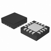
16-TFQFN Exposed Pad
Lead Free Status / RoHS Status
Lead free / RoHS Compliant
Number Of Bits
-


1. In the differential configuration when the input termination pin (V
2. All V
Table 3. PIN DESCRIPTION
Pin
signal is applied on IN/IN input, then the device will be susceptible to self−oscillation. Q/Q outputs have internal 50 W source termination
resistor.
10
11
12
13
14
15
16
1
2
3
4
5
6
7
8
9
CC,
V
SCLKOUT
CCD
SCLKIN
SDOUT
SLOAD
Name
VCCD
SDIN
GND
GND
VCC
VCC
VCC
EP
VT
IN
IN
Q
Q
and GND pins must be externally connected to a power supply voltage to guarantee proper device operation.
LVPECL, CML,
LVPECL, CML,
LVCMOS Input
LVCMOS Input
LVCMOS Input
LVDS Input
LVDS Input
LVCMOS
LVCMOS
Output
Output
CML
CML
I/O
−
−
−
−
−
−
GND
VT
IN
IN
Figure 4. Pin Configuration (Top View)
Internal 50−W Termination Pin for IN and IN
Non−inverted Differential Clock/Data Input. (Note 1)
Inverted Differential Clock/Data Input. (Note 1)
Negative Supply Voltage; (Note 2)
Positive Supply Voltage for Serial Bus Logic and 5−Bit DAC; (Note 2)
Serial Data Out
Serial Clock Out
Negative Supply Voltage; (Note 2)
Positive Supply Voltage for the analog circuitry and CML Output buffer; (Note 2)
Inverted Differential Output. (Note 1)
Non−inverted Differential Output. (Note 1)
Positive Supply Voltage for the analog circuitry and CML Output buffer; (Note 2)
When the SLOAD pin is LOW or left open (has internal pulldown resistor), the output of
the shift register will input the 4−bit DAC and set the EQEN bit. When HIGH, the input to
the 4−bit DAC is locked to the state prior to when SLOAD went HIGH.
Serial Clock In; pin will default LOW when left open (has internal pulldown resistor)
Serial Data In; pin will default LOW when left open (has internal pulldown resistor)
Positive Supply Voltage for the analog circuitry and CML Output buffer; (Note 2)
The Exposed Pad (EP) on the QFN−16 package bottom is thermally connected to the die
for improved heat transfer out of package. The exposed pad must be attached to a heat−
sinking conduit. The pad is also electrically connected to the die, and must be electrically
and thermally connected to GND on the PC board.
1
2
3
4
16
5
http://onsemi.com
NB7VPQ16M
15
6
T
) is connected to a common termination voltage or left open, and if no input
4
14
7
13
8
12
10
11
9
Description
V
Q
Q
V
CC
CC
Exposed Pad (EP)
Related parts for NB7VPQ16MMNHTBG
Image
Part Number
Description
Manufacturer
Datasheet
Request
R

Part Number:
Description:
1.8v / 2.5v Cml 12.5 Gbps Programmable Pre-emphasis Copper/cable Driver With Selectable Equalizer Receiver
Manufacturer:
ON Semiconductor
Datasheet:
Part Number:
Description:
ON Semiconductor [VOLTAGE REGULATOR]
Manufacturer:
ON Semiconductor
Datasheet:
Part Number:
Description:
357-036-542-201 CARDEDGE 36POS DL .156 BLK LOPRO
Manufacturer:
ON Semiconductor
Datasheet:
Part Number:
Description:
357-036-542-201 CARDEDGE 36POS DL .156 BLK LOPRO
Manufacturer:
ON Semiconductor
Datasheet:
Part Number:
Description:
357-036-542-201 CARDEDGE 36POS DL .156 BLK LOPRO
Manufacturer:
ON Semiconductor
Datasheet:
Part Number:
Description:
357-036-542-201 CARDEDGE 36POS DL .156 BLK LOPRO
Manufacturer:
ON Semiconductor
Datasheet:
Part Number:
Description:
357-036-542-201 CARDEDGE 36POS DL .156 BLK LOPRO
Manufacturer:
ON Semiconductor
Datasheet:
Part Number:
Description:
357-036-542-201 CARDEDGE 36POS DL .156 BLK LOPRO
Manufacturer:
ON Semiconductor
Datasheet:
Part Number:
Description:
357-036-542-201 CARDEDGE 36POS DL .156 BLK LOPRO
Manufacturer:
ON Semiconductor
Datasheet:
Part Number:
Description:
357-036-542-201 CARDEDGE 36POS DL .156 BLK LOPRO
Manufacturer:
ON Semiconductor
Datasheet:
Part Number:
Description:
357-036-542-201 CARDEDGE 36POS DL .156 BLK LOPRO
Manufacturer:
ON Semiconductor
Datasheet:
Part Number:
Description:
357-036-542-201 CARDEDGE 36POS DL .156 BLK LOPRO
Manufacturer:
ON Semiconductor
Datasheet:
Part Number:
Description:
Manufacturer:
ON Semiconductor
Datasheet:
Part Number:
Description:
Manufacturer:
ON Semiconductor
Datasheet: