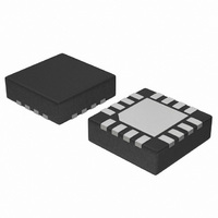
NB7VPQ16MMNHTBG ON Semiconductor, NB7VPQ16MMNHTBG Datasheet - Page 7

NB7VPQ16MMNHTBG
Manufacturer Part Number
NB7VPQ16MMNHTBG
Description
IC CML DVR PRE-EMPH 1CH 16-QFN
Manufacturer
ON Semiconductor
Datasheet
1.NB7VPQ16MMNTXG.pdf
(16 pages)
Specifications of NB7VPQ16MMNHTBG
Logic Type
CML Driver with Selectable Equalizer Receiver
Supply Voltage
1.71 V ~ 2.625 V
Operating Temperature
-40°C ~ 85°C
Mounting Type
Surface Mount
Package / Case
16-TFQFN Exposed Pad
Lead Free Status / RoHS Status
Lead free / RoHS Compliant
Number Of Bits
-
NOTE: Device will meet the specifications after thermal equilibrium has been established when mounted in a test socket or printed circuit
8. Measured using a 400 mV source, 50% duty cycle clock source. All output loading with external 50 W to V
9. Input / Output voltage swing is a single−ended measurement operating in differential mode.
10. V
11. Additive RMS jitter with 50% duty cycle Clock signal.
12. Peak−to−Peak jitter with input NRZ data at PRBS23.
Table 7. AC CHARACTERISTICS
f
f
f
VOD
t
V
t
t
t
t
t
t
t
t
t
t
t
V
t
DATAMAX
MAX
SCLKIN
PE
PLH
PHL
DC
s1
s2
s3
h1
h2
h3
PW_SLOAD
JITTER
r
, t
Symbol
CMR
INPP
(20% − 80%); PE = 0 dB, EQEN = 0
input signal.
f
CMR
,
0dB
board with maintained transverse airflow greater than 500 lfpm. Electrical parameters are guaranteed only over the declared
operating temperature range. Functional operation of the device exceeding these conditions is not implied. Device specification limit
values are applied individually under normal operating conditions and not valid simultaneously.
min varies 1:1 with GND, V
Maximum Input Clock Frequency (Note 9)
Serial Clock Input Frequency
Maximum Input Data Rate
Output Voltage Amplitude (see Table 1)
(@ V
Pre−Emphasis Width, tested at −12dB Pre−Emphasis
Input Common Mode Range (Differential Configuration, Note 10) (Figure 8)
Propagation Delay to Differential Outputs,
1 GHz, measured at differential cross−point
Output Clock Duty Cycle (Reference Duty Cycle = 50%)
Setup Time @ 50 MHz (Figures 9 and 10)
Hold Time @ 50 MHz (Figures 9 and 10)
SLOAD Minimum Pulse Width (Figure 10)
RJ – Output Random Jitter (Note 11) f
DJ − Residual Output Deterministic Jitter (Note 12)
Input Voltage Swing (Differential Configuration) (Note 9)
Output Rise/Fall Times @ 1 GHz (20% − 80%), Q, Q
INPPmin
) (See Figure 3, Note 9)
CMR
V
max varies 1:1 with V
CC
(EQ = 0, PE = 0 dB) FR4 v 3”, f v 12.5 Gbps
= V
Characteristic
(Figures 15 and 16) FR4 = 12”, f v 6.5 Gbps
V
IN
IN
CCD
T
50 W
50 W
= 1.71 V to 2.625 V; GND = 0 V; T
in
Figure 5. Input Structure
v 8.0 GHz
http://onsemi.com
CC
. The V
V
OUTPP
SCLKIN to SCLKOUT
7
V
SCLKIN to SLOAD
SCLKIN to SLOAD
CC
CMR
SDIN to SCLKIN
SDIN to SCLKIN
SLOAD to IN/IN
w 200 mV
f
f
f
range is referenced to the most positive side of the differential
in
in
in
IN/IN to Q/Q
v 6.0 GHz
v 8.0 GHz
v 5.0 GHz
A
= −40°C to 85°C (Note 8)
1050
12.5
Min
300
200
150
100
45
10
8
5
5
1
2
6
Typ
400
300
130
200
0.1
14
50
35
5
CC
. Input edge rates 40 ps.
1200
Max
V
250
0.8
20
10
55
10
10
50
CC
ps pk−pk
ps rms
Gbps
GHz
MHz
Unit
mV
mV
mV
ps
ps
ns
ns
ns
ns
ps
%


