SSTUA32864EC,551 NXP Semiconductors, SSTUA32864EC,551 Datasheet
SSTUA32864EC,551
Specifications of SSTUA32864EC,551
SSTUA32864EC-S
SSTUA32864EC-S


Related parts for SSTUA32864EC,551


SSTUA32864EC,551 Summary of contents
Page 1
SSTUA32864 1.8 V configurable registered buffer for DDR2-667 RDIMM applications Rev. 02 — 9 March 2007 1. General description The SSTUA32864 is a 25-bit 14-bit configurable registered buffer designed for 1 ...
Page 2
... NXP Semiconductors 2. Features I Configurable register supporting DDR2 Registered DIMM applications I Configurable to 25-bit mode or 14-bit mode I Controlled output impedance drivers enable optimal signal integrity and speed I Exceeds SSTUA32864 JEDEC specification speed performance (1.8 ns max. single-bit switching propagation delay; 2.0 ns max. mass-switching) ...
Page 3
... NXP Semiconductors 5. Functional diagram (1) Disabled configuration. Fig 1. Functional diagram of SSTUA32864 mode (positive logic) SSTUA32864_2 Product data sheet 1.8 V configurable registered buffer for DDR2-667 RDIMM applications RESET CK CK VREF DCKE DODT DCS CSR D1 to other channels Rev. 02 — 9 March 2007 ...
Page 4
... NXP Semiconductors 6. Pinning information 6.1 Pinning Fig 2. Pin configuration for LFBGA96 Fig 3. Ball mapping register ( 0); top view SSTUA32864_2 Product data sheet 1.8 V configurable registered buffer for DDR2-667 RDIMM applications SSTUA32864EC/G ball A1 SSTUA32864EC index area Transparent top view DCKE n.c. ...
Page 5
... NXP Semiconductors Fig 4. Ball mapping register A ( 1); top view Fig 5. Ball mapping register B ( 1); top view SSTUA32864_2 Product data sheet 1.8 V configurable registered buffer for DDR2-667 RDIMM applications DCKE n.c. VREF B D2 DNU GND C D3 DNU DODT n.c. GND E D5 ...
Page 6
... NXP Semiconductors 6.2 Pin description Table 2. Pin description Symbol Pin GND B3, B4, D3, D4, F3, F4, H3, H4, K3, K4, M3, M4, P3 A4, C3, C4, E3, E4, DD G3, G4, J3, J4, L3, L4, N3, N4, R3, R4, T4 VREF A3, T3 ZOH J5 ZOL C0, C1 G6, G5 RESET G2 CSR, DCS J2 D25 [1] DODT [1] DCKE [ Q25, Q1A to Q14A, ...
Page 7
... NXP Semiconductors 7. Functional description 7.1 Function table Table LOW voltage level HIGH voltage level don’t care; = HIGH-to-LOW transition RESET [ the previous state of the associated output. 0 SSTUA32864_2 Product data sheet 1.8 V configurable registered buffer for DDR2-667 RDIMM applications Function table (each flip-flop) ...
Page 8
... NXP Semiconductors 8. Limiting values Table 4. Limiting values In accordance with the Absolute Maximum Rating System (IEC 60134). Symbol Parameter V supply voltage DD V input voltage I V output voltage O I input clamping current IK I output clamping current OK I output current O I continuous current through ...
Page 9
... NXP Semiconductors 10. Characteristics Table 6. Characteristics Recommended operating conditions; T unless otherwise specified. Symbol Parameter V HIGH-level output voltage OH V LOW-level output voltage OL I input current I I supply current DD I dynamic operating current DDD per MHz C input capacitance i SSTUA32864_2 Product data sheet 1.8 V configurable registered buffer for DDR2-667 RDIMM applications = +70 C ...
Page 10
... NXP Semiconductors Table 7. Timing requirements Recommended operating conditions; T See Figure 6 through Figure 11. Symbol Parameter f clock frequency clock t pulse width W t differential inputs active time ACT t differential inputs inactive time INACT t set-up time su t hold time h [1] This parameter is not necessarily production tested. ...
Page 11
... NXP Semiconductors 11. Test information 11.1 Test circuit All input pulses are supplied by generators having the following characteristics: PRR 10 MHz; Z The outputs are measured one at a time with one transition per measurement. CK inputs (1) C Fig 6. Load circuit (1) I Fig 7. Voltage and current waveforms; inputs active and inactive times Fig 8. Voltage waveforms ...
Page 12
... NXP Semiconductors Fig 9. Voltage waveforms; setup and hold times Fig 10. Voltage waveforms; propagation delay times (clock to output) Fig 11. Voltage waveforms; propagation delay times (reset to output) SSTUA32864_2 Product data sheet 1.8 V configurable registered buffer for DDR2-667 RDIMM applications input V ref V = 600 mV ...
Page 13
... NXP Semiconductors 11.2 Output slew rate measurement All input pulses are supplied by generators having the following characteristics: PRR 10 MHz; Z (1) C Fig 12. Load circuit, HIGH-to-LOW slew measurement Fig 13. Voltage waveforms, HIGH-to-LOW slew rate measurement (1) C Fig 14. Load circuit, LOW-to-HIGH slew measurement Fig 15 ...
Page 14
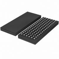
... NXP Semiconductors 12. Package outline LFBGA96: plastic low profile fine-pitch ball grid array package; 96 balls; body 13.5 x 5.5 x 1.05 mm ball A1 index area ball A1 index area DIMENSIONS (mm are the original dimensions) A UNIT max. 0.41 1.2 0.51 mm 1.5 0.31 0.9 0.41 OUTLINE VERSION IEC SOT536-1 Fig 16 ...
Page 15
... NXP Semiconductors 13. Soldering This text provides a very brief insight into a complex technology. A more in-depth account of soldering ICs can be found in Application Note AN10365 “Surface mount reflow soldering description” . 13.1 Introduction to soldering Soldering is one of the most common methods through which packages are attached to Printed Circuit Boards (PCBs), to form electrical circuits ...
Page 16
... NXP Semiconductors 13.4 Reflow soldering Key characteristics in reflow soldering are: • Lead-free versus SnPb soldering; note that a lead-free reflow process usually leads to higher minimum peak temperatures (see reducing the process window • Solder paste printing issues including smearing, release, and adjusting the process window for a mix of large and small components on one board • ...
Page 17
... NXP Semiconductors Fig 17. Temperature profiles for large and small components For further information on temperature profiles, refer to Application Note AN10365 “Surface mount reflow soldering description” . 14. Abbreviations Table 12. Acronym CMOS DDR DIMM LVCMOS PRR RDIMM SSTL SSTUA32864_2 Product data sheet 1.8 V confi ...
Page 18
... Release date SSTUA32864_2 20070309 • Modifications: The format of this data sheet has been redesigned to comply with the new identity guidelines of NXP Semiconductors. • Legal texts have been adapted to the new company name where appropriate. • Table 4 “Limiting – changed Parameter for V – ...
Page 19
... For detailed and full information see the relevant full data sheet, which is available on request via the local NXP Semiconductors sales office. In case of any inconsistency or conflict with the short data sheet, the full data sheet shall prevail ...
Page 20
... NXP Semiconductors 18. Contents 1 General description . . . . . . . . . . . . . . . . . . . . . . 1 2 Features . . . . . . . . . . . . . . . . . . . . . . . . . . . . . . . 2 3 Applications . . . . . . . . . . . . . . . . . . . . . . . . . . . . 2 4 Ordering information . . . . . . . . . . . . . . . . . . . . . 2 5 Functional diagram . . . . . . . . . . . . . . . . . . . . . . 3 6 Pinning information . . . . . . . . . . . . . . . . . . . . . . 4 6.1 Pinning . . . . . . . . . . . . . . . . . . . . . . . . . . . . . . . 4 6.2 Pin description . . . . . . . . . . . . . . . . . . . . . . . . . 6 7 Functional description . . . . . . . . . . . . . . . . . . . 7 7.1 Function table . . . . . . . . . . . . . . . . . . . . . . . . . . 7 8 Limiting values Recommended operating conditions Characteristics . . . . . . . . . . . . . . . . . . . . . . . . . . 9 11 Test information . . . . . . . . . . . . . . . . . . . . . . . . 11 11.1 Test circuit ...