SSTU32866EC/G,557 NXP Semiconductors, SSTU32866EC/G,557 Datasheet - Page 27
SSTU32866EC/G,557
Manufacturer Part Number
SSTU32866EC/G,557
Description
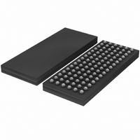
IC BUFFER 1.8V 25BIT SOT536-1
Manufacturer
NXP Semiconductors
Datasheet
1.SSTU32866ECG551.pdf
(29 pages)
Specifications of SSTU32866EC/G,557
Logic Type
1:1, 1:2 Configurable Registered Buffer with Parity
Supply Voltage
1.7 V ~ 1.9 V
Number Of Bits
25, 14
Operating Temperature
0°C ~ 70°C
Mounting Type
Surface Mount
Package / Case
96-LFBGA
Logic Family
SSTU
Logical Function
Registered Buffer
Number Of Elements
1
Number Of Inputs
25
Number Of Outputs
25
High Level Output Current
-8mA
Low Level Output Current
8mA
Propagation Delay Time
3ns
Operating Supply Voltage (typ)
1.8V
Operating Supply Voltage (max)
1.9V
Operating Supply Voltage (min)
1.7V
Clock-edge Trigger Type
Posit/Negat-Edge
Polarity
Non-Inverting
Technology
CMOS
Frequency (max)
450(Min)MHz
Mounting
Surface Mount
Pin Count
96
Operating Temp Range
0C to 70C
Operating Temperature Classification
Commercial
Lead Free Status / RoHS Status
Lead free / RoHS Compliant
Other names
935275473557
SSTU32866EC/G
SSTU32866EC/G
SSTU32866EC/G
SSTU32866EC/G


Philips Semiconductors
15. Revision history
Table 13:
9397 750 14181
Product data sheet
Document ID
SSTU32866_2
Modifications:
SSTU32866-01
Revision history
Release date
20041111
20040709
•
•
•
•
•
•
•
•
•
•
•
•
•
•
The format of this data sheet has been redesigned to comply with the new presentation and
information standard of Philips Semiconductors.
Data sheet status upgraded to ‘Product data sheet’.
(Old) Figure 1 and Figure 2 (logic diagrams) moved to
Section 6 “Pinning information”
– changed ‘NC’ to ‘n.c.’ and ‘DNU’ to ‘d.n.u.’
– added
– added
–
Table 3 “Function table (each
Table 4 “Parity and standby function
– added (new)
–
Table 5 “Limiting
– symbol V
– symbols ESD
Table 6 “Recommended operating
– changed column heading from ‘Nom’ to ‘Typ’
– changed V
– changed V
– table note split into 2 notes; references added.
merged sections “Static characteristics” and “Dynamic characteristics” into
“Characteristics”
Table 7
“dynamic operating current per MHz ...”; change Unit from “ A/MHz” to “ A”.
Table 8 “Timing
– changed symbol f
– changed symbol t
– changed symbol t
Figure 7
Section 11.1 “Parameter measurement information for data output load
Figure 14
added
Table 2 “Pin
added pin number column.
Table note
‘data inputs (Dn) ...’
‘data inputs (Dn)
Section
“Characteristics”: changed I
modified.
Figure 3 “Pin configuration for LFBGA96”
Figure
and
Data sheet status
Product data sheet
Objective data
i
changed to V
IH
IL
[4]: changed ‘This transition assumes ...’ to ‘This condition assumes ...’.
Figure 15
14.
description”: added (new)
requirements”:
(for Data, CSR, and PAR_IN inputs) to V
(for Data, CSR, and PAR_IN inputs) to V
Table note [1]
HBM
values”:
4,
Figure
Rev. 02 — 11 November 2004
CLOCK
SU
H
and ESD
to t
to t
modified.
h
5, and
I
su
; Symbol V
to f
flip-flop)”: added
MM
and its reference at ‘Outputs’.
clock
1.8 V DDR2 configurable registered buffer with parity
Figure 6
replaced with V
conditions”:
DDD
table”:
Change notice
-
-
o
Parameter from “dynamic operating current ...” to
changed to V
Table note [1]
(replacing old Tables 2, 3 and 4 “Ball mapping”)
Table note [1]
esd
(added model types under “Conditions”)
O
Section 5 “Functional diagram”
.
Doc. number
9397 750 14181
9397 750 12145
and its references at affected pins.;
IH(AC)
IL(AC)
and its reference at ‘Outputs’.
and V
and V
© Koninklijke Philips Electronics N.V. 2004. All rights reserved.
IL(DC)
IH(DC)
SSTU32866
circuit”: titles for
; condition changed to
; condition changed to
Supersedes
SSTU32866-01
-
Section 10
27 of 29
Related parts for SSTU32866EC/G,557
Image
Part Number
Description
Manufacturer
Datasheet
Request
R

Part Number:
Description:
NXP Semiconductors designed the LPC2420/2460 microcontroller around a 16-bit/32-bitARM7TDMI-S CPU core with real-time debug interfaces that include both JTAG andembedded trace
Manufacturer:
NXP Semiconductors
Datasheet:

Part Number:
Description:
NXP Semiconductors designed the LPC2458 microcontroller around a 16-bit/32-bitARM7TDMI-S CPU core with real-time debug interfaces that include both JTAG andembedded trace
Manufacturer:
NXP Semiconductors
Datasheet:
Part Number:
Description:
NXP Semiconductors designed the LPC2468 microcontroller around a 16-bit/32-bitARM7TDMI-S CPU core with real-time debug interfaces that include both JTAG andembedded trace
Manufacturer:
NXP Semiconductors
Datasheet:
Part Number:
Description:
NXP Semiconductors designed the LPC2470 microcontroller, powered by theARM7TDMI-S core, to be a highly integrated microcontroller for a wide range ofapplications that require advanced communications and high quality graphic displays
Manufacturer:
NXP Semiconductors
Datasheet:
Part Number:
Description:
NXP Semiconductors designed the LPC2478 microcontroller, powered by theARM7TDMI-S core, to be a highly integrated microcontroller for a wide range ofapplications that require advanced communications and high quality graphic displays
Manufacturer:
NXP Semiconductors
Datasheet:
Part Number:
Description:
The Philips Semiconductors XA (eXtended Architecture) family of 16-bit single-chip microcontrollers is powerful enough to easily handle the requirements of high performance embedded applications, yet inexpensive enough to compete in the market for hi
Manufacturer:
NXP Semiconductors
Datasheet:
Part Number:
Description:
The XA-S3 device is a member of Philips Semiconductors? XA(eXtended Architecture) family of high performance 16-bitsingle-chip microcontrollers
Manufacturer:
NXP Semiconductors
Datasheet:

Part Number:
Description:
The NXP BlueStreak LH75401/LH75411 family consists of two low-cost 16/32-bit System-on-Chip (SoC) devices
Manufacturer:
NXP Semiconductors
Datasheet:
Part Number:
Description:
The NXP LPC3130/3131 combine an 180 MHz ARM926EJ-S CPU core, high-speed USB2
Manufacturer:
NXP Semiconductors
Datasheet:
Part Number:
Description:
The NXP LPC3141 combine a 270 MHz ARM926EJ-S CPU core, High-speed USB 2
Manufacturer:
NXP Semiconductors
Part Number:
Description:
The NXP LPC3143 combine a 270 MHz ARM926EJ-S CPU core, High-speed USB 2
Manufacturer:
NXP Semiconductors

Part Number:
Description:
The NXP LPC3152 combines an 180 MHz ARM926EJ-S CPU core, High-speed USB 2
Manufacturer:
NXP Semiconductors
Part Number:
Description:
The NXP LPC3154 combines an 180 MHz ARM926EJ-S CPU core, High-speed USB 2
Manufacturer:
NXP Semiconductors

Part Number:
Description:
Standard level N-channel enhancement mode Field-Effect Transistor (FET) in a plastic package using NXP High-Performance Automotive (HPA) TrenchMOS technology
Manufacturer:
NXP Semiconductors
Datasheet: