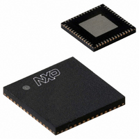
SSTV16859BS,118 NXP Semiconductors, SSTV16859BS,118 Datasheet - Page 6

SSTV16859BS,118
Manufacturer Part Number
SSTV16859BS,118
Description
IC REG BUFFER 26BIT 56HVQFN
Manufacturer
NXP Semiconductors
Series
SSTr
Datasheet
1.SSTV16859BS118.pdf
(14 pages)
Specifications of SSTV16859BS,118
Logic Type
Registered Buffer for DDR
Supply Voltage
2.3 V ~ 2.7 V
Number Of Bits
13, 26
Operating Temperature
0°C ~ 70°C
Mounting Type
Surface Mount
Package / Case
56-VQFN Exposed Pad, 56-HVQFN, 56-SQFN, 56-DHVQFN
Logic Family
SSTV
Logical Function
Registered Buffer
Number Of Elements
1
Number Of Inputs
13
Number Of Outputs
26
High Level Output Current
-20mA
Low Level Output Current
20mA
Propagation Delay Time
2.4ns
Operating Supply Voltage (typ)
2.5V
Operating Supply Voltage (max)
2.7V
Operating Supply Voltage (min)
2.3V
Clock-edge Trigger Type
Posit/Negat-Edge
Polarity
Non-Inverting
Technology
CMOS
Frequency (max)
200(Min)MHz
Mounting
Surface Mount
Pin Count
56
Operating Temp Range
0C to 70C
Operating Temperature Classification
Commercial
Lead Free Status / RoHS Status
Lead free / RoHS Compliant
Other names
935271266118
SSTV16859BS-T
SSTV16859BS-T
SSTV16859BS-T
SSTV16859BS-T
1. Stresses beyond those listed under “absolute maximum ratings” may cause permanent damage to the device. These are stress ratings
2. The input and output negative-voltage ratings may be exceeded if the input and output current ratings are observed.
3. This value is limited to 3.6 V maximum.
4. The performance capability of a high-performance integrated circuit in conjunction with its thermal environment can create junction
1. The RESET input of the device must be held at V
Philips Semiconductors
ABSOLUTE MAXIMUM RATINGS
NOTES:
RECOMMENDED OPERATING CONDITIONS
NOTE:
2002 Feb 19
SYMBOL
SYMBOL
SYMBOL
2.5 V 13-bit to 26-bit SSTL_2
registered buffer for stacked DDR DIMM
only and functional operation of the device at these or any other conditions beyond those indicated under “recommended operating
conditions” is not implied. Exposure to absolute-maximum-rated conditions for extended periods may affect device reliability.
temperatures that are detrimental to reliability. The maximum junction temperature of this integrated circuit should not exceed 150 C.
unless RESET is low.
V
V
T
V
V
V
T
V
V
V
V
I
I
V
V
V
I
V
REF
amb
I
OK
I
V
OH
OL
V
ICR
stg
DD
DD
IK
TT
O
IH
IH
IH
ID
IL
IL
IL
O
I
I
Operating free-air temperature range
Continuous current through each
Storage temperature range
Continuous output current
AC HIGH-level input voltage
DC HIGH-level input voltage
DC LOW-level input voltage
AC LOW-level input voltage
Common-mode input range
HIGH-level output current
Supply voltage range
Output voltage range
Output clamp current
LOW-level output current
HIGH-level input voltage
Differential input voltage
LOW-level input voltage
Input voltage range
Input clamp current
Termination voltage
Reference voltage
PARAMETER
PARAMETER
V
(V
Supply voltage
PARAMETER
DD
Input voltage
REF
or GND
= V
DD
/2)
1
DD
or GND to ensure proper device operation. The differential inputs must not be floating,
1
CONDITIONS
Data inputs
Data inputs
Data inputs
Data inputs
RESET
CK, CK
CK, CK
V
V
O
6
I
Notes 2 and 3
Notes 2 and 3
V
CONDITION
CONDITION
< 0 or V
< 0 or V
O
= 0 to V
I
O
> V
> V
DD
V
V
V
DD
REF
REF
REF
DD
1.15
0.97
MIN
V
+ 310 mV
+ 150 mV
360
1.7
0.0
– 40 mV
—
—
—
—
DD
0
0
V
TYP
1.25
—
REF
—
—
—
—
—
—
—
—
—
—
—
—
–0.5
–0.5
–0.5
MIN
–65
—
—
—
—
V
V
V
REF
REF
REF
LIMITS
SSTV16859
MAX
1.35
1.53
V
V
– 310 mV
– 150 mV
–20
+70
V
V
2.7
0.7
+ 40 mV
20
—
—
—
DD
DD
DD
DD
MAX
+150
+3.6
100
50
50
50
+ 0.5
+ 0.5
Product data
UNIT
UNIT
UNIT
mV
mA
mA
mA
mA
mA
mA
V
V
V
V
V
V
V
V
V
V
V
V
V
V
C
C


