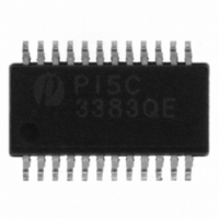
PI5C3383QE Pericom Semiconductor, PI5C3383QE Datasheet - Page 3

PI5C3383QE
Manufacturer Part Number
PI5C3383QE
Description
IC 5-BIT 4-PORT BUS SW 24-QSOP
Manufacturer
Pericom Semiconductor
Type
Bus FET Exchange Switchr
Datasheet
1.PI5C3383QE.pdf
(4 pages)
Specifications of PI5C3383QE
Circuit
5 x 1:1
Independent Circuits
1
Voltage Supply Source
Single Supply
Operating Temperature
-40°C ~ 85°C
Mounting Type
Surface Mount
Package / Case
24-QSOP
Lead Free Status / RoHS Status
Lead free / RoHS Compliant
Voltage - Supply
-
Current - Output High, Low
-
Lead Free Status / Rohs Status
Compliant
Power Supply Characteristics
Switching Characteristics over Operating Range
Applications
Logic Inputs
The logic control inputs can be driven up to +5.5V regardless of the supply voltage. For example, given a 5.0V supply, the control or
select pins may be driven low to 0V and high to 5.5V. Driving the control or select pins Rail-to-Rail
Power-Supply Sequencing
Proper power-supply sequencing is recommended for all CMOS devices. Always apply VCC before applying signals to the input/
output or control pins.
Rail-to-Rail is a registered trademark of Nippon Motorola, Ltd.
Notes:
1.
2.
3.
4.
Notes:
1.
2.
Parameters
Parameters
For Max. or Min. conditions, use appropriate value specifi ed under Electrical Characteristics for the applicable device.
Typical values are at Vcc = 5.0V, +25°C ambient.
Per TTL driven input (V
This current applies to the control inputs only and represent the current required to switch internal capacitance at the specifi ed frequency. The
A, B, C, and D inputs generate no signifi cant AC or DC currents as they transition. This parameter is not tested, but is guaranteed by design.
This parameter is guaranteed but not tested on Propagation Delays.
The bus switch contributes no propagational delay other than the RC delay of the On-Resistance of the switch and the load capacitance. The
time constant for the switch alone is of the order of 0.25ns for 50pF load. Since this time constant is much smaller than the rise/fall times of
typical driving signals, it adds very little propagational delay to the system. Propagational delay of the bus switch when used in a system is
determined by the driving circuit on the driving side of the switch and its interaction with the load on the driven side.
∆I
I
t
t
t
t
I
t
t
CCD
t
PLH
PHL
PZH
PHZ
PLZ
CC
PZL
BX
CC
06-0226
Quiescent Power
Supply Current
Supply Current per
Input @ TTL HIGH
Supply Current per
Input per MHz
Propagation Delay
Bus Enable Time BE to Cx or Dx
Bus Disable Time BE to Cx or Dx
Bus Exchange Time BX to Cx or Dx
Description
IN
= 3.4V, control inputs only); A, B, C, and D pins do not contribute to Icc.
(4)
Description
(1,2)
Ax to Cx, Bx to Dx
V
V
V
AB and CD pins Open
BE = GND
Control Input Toggling
50% Duty Cycle
CC
CC
CC
= Max.
= Max.
= Max.
Test Conditions
3
Condidtions
R
C
L
L
= 500Ω
= 50pF
V
V
IN
IN
(1)
= GND or V
= 3.4V
(3)
5-Bit, 4-Port Bus Exchange Switch
Min.
CC
1.5
1.5
1.5
Min.
®
minimizes power con sump tion.
Com
Typ.
0.25
Typ.
0.1
(2)
Max
6.5
5.5
6.5
Max.
0.25
PS7028J
3.0
2.5
PI5C3383
Units
Units
MHz
mA/
mA
ns
μA
05/02/07


