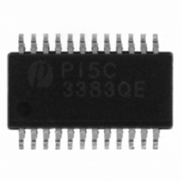
PI5C3383QE Pericom Semiconductor, PI5C3383QE Datasheet - Page 2

PI5C3383QE
Manufacturer Part Number
PI5C3383QE
Description
IC 5-BIT 4-PORT BUS SW 24-QSOP
Manufacturer
Pericom Semiconductor
Type
Bus FET Exchange Switchr
Datasheet
1.PI5C3383QE.pdf
(4 pages)
Specifications of PI5C3383QE
Circuit
5 x 1:1
Independent Circuits
1
Voltage Supply Source
Single Supply
Operating Temperature
-40°C ~ 85°C
Mounting Type
Surface Mount
Package / Case
24-QSOP
Lead Free Status / RoHS Status
Lead free / RoHS Compliant
Voltage - Supply
-
Current - Output High, Low
-
Lead Free Status / Rohs Status
Compliant
DC Electrical Characteristics
Capacitance
Notes:
1.
2.
3.
4.
Notes:
1.
Maximum Ratings
(Above which the useful life may be impaired. For user guidelines, not tested.)
Parameters
Storage Temperature ..........................................................–65°C to +150°C
Ambient Temperature with Power Applied .........................–40°C to +85°C
Supply Voltage to Ground Potential (Inputs & V
Supply Voltage to Ground Potential (Outputs & D/O Only) –0.5V to +7.0V
DC Input Voltage ..................................................................–0.5V to +7.0V
DC Output Current ............................................................................120 mA
Power Dissipation .................................................................................0.5W
Parameters
V
V
I
I
I
V
I
V
R
For Max. or Min. conditions, use appropriate value specifi ed under Electrical Characteristics for the applicable device type.
Typical values are at V
Not more than one output should be shorted at one time. Duration of the test should not exceed one second.
Measured by the voltage drop between AB and CD pin at indicated current through the switch. On-Resistance is determined by the lower of
the voltages on the two (A or B, C or D) pins.
This parameter is determined by device characterization but is not production tested.
IH
IL
OZ
OS
ON
IH
IL
IK
H
C
C
C
06-0226
OFF
ON
IN
(1)
(T
Input HIGH Voltage
Input LOW Voltage
Input HIGH Current
Input LOW Current
High Impedance Output Current
Clamp Diode Voltage
Short Circut Current
Input Hysteresis at Control Pins
Switch On-Resistance
A
Description
= 25°C, f = 1 MHz)
Input Capacitance
AB/CD Capacitance, Switch OFF
AB/CD Capacitance, Switch ON
CC
= 5.0V, T
A
(3)
= 25°C ambient and maximum loading.
(Over the Operating Range, T
(4)
Description
CC
Only) ...–0.5V to +7.0V
Test Condidtions
Guaranteed Logic HIGH Level
Guaranteed Logic LOW Level
V
V
0 ≤ A B, CD ≤ V
V
AB (CD) = 0V, CD (AB) = V
V
V
CC
CC
CC
CC
CC
=Min., I
= Max., V
= Max., V
= Min., V
= Min., V
2
IN
A
IN
IN
IN
IN
= –40°C to +85°C, V
= –18mA
CC
= 0.0V, I
= 2.4V, I
(1)
= V
= GND
CC
Test Conditions
Note:
Stresses greater than those listed under MAXIMUM RAT-
INGS may cause permanent damage to the de vice. This is a
stress rating only and functional op er a tion of the device at
these or any other conditions above those indicated in the
operational sections of this spec i fi ca tion is not implied. Ex-
po sure to absolute maximum rating conditions for extended
periods may affect reliability.
ON
ON
V
CC
= 48mA
= 15mA
IN
= 0V
5-Bit, 4-Port Bus Exchange Switch
CC
= 5V ±5%)
Min. Typ.
–0.5
100
2.0
Typ.
14
6
8
150
10
5
(2)
Units
pF
PS7028J
Max
–0.7
0.8
±1
±1
±1
15
7
PI5C3383
Units
–1.2
mA
mV
μA
05/02/07
V
Ω


