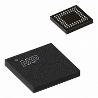
CBTV4010EE,557 NXP Semiconductors, CBTV4010EE,557 Datasheet - Page 5

CBTV4010EE,557
Manufacturer Part Number
CBTV4010EE,557
Description
IC 10BIT 1:4 BUS SWITCH 64-TFBGA
Manufacturer
NXP Semiconductors
Series
CBTr
Type
Bus Switchr
Datasheet
1.CBTV4010EE557.pdf
(10 pages)
Specifications of CBTV4010EE,557
Package / Case
64-TFBGA
Circuit
10 x 1:4
Independent Circuits
1
Voltage Supply Source
Single Supply
Voltage - Supply
2.3 V ~ 2.7 V
Operating Temperature
0°C ~ 85°C
Mounting Type
Surface Mount
Maximum Data Rate
0.4 Gbps
Minimum Operating Temperature
0 C
Mounting Style
SMD/SMT
Number Of Clock Inputs
10
Supply Voltage (max)
2.7 V
Supply Voltage (min)
2.3 V
Maximum Operating Temperature
+ 85 C
Lead Free Status / RoHS Status
Lead free / RoHS Compliant
Current - Output High, Low
-
Lead Free Status / RoHS Status
Lead free / RoHS Compliant, Lead free / RoHS Compliant
Other names
935271264557
CBTV4010EE
CBTV4010EE
CBTV4010EE
CBTV4010EE
Available stocks
Company
Part Number
Manufacturer
Quantity
Price
Company:
Part Number:
CBTV4010EE,557
Manufacturer:
NXP Semiconductors
Quantity:
10 000
1. The propagation delay is based on the RC time constant of the typical on–state resistance of the switch and a load capacitance, when driven
1. All typical values are at V
2. Measured by the current between the Host and the DIMM terminals at the indicated voltages on each side of the switch.
3. Capacitance values are measured at a of 10 MHz and a bias voltage 3 V. Capacitance is not production tested.
2. Skew is not production tested.
Philips Semiconductors
DC ELECTRICAL CHARACTERISTICS
NOTES:
AC CHARACTERISTICS
NOTES:
2002 Feb 19
SYMBOL
SYMBOL
SYMBOL
10-bit DDR SDRAM mux/bus switch
by an ideal voltage source (zero output impedance); 20
This parameter is not production tested.
t
t
C
r
r
t
t
t
V
I
C
osk
esk
on
pd
en
dis
CC
I
on
IK
I
in
2
2
Propagation delay
enable
disable
Output skew
Any output to any output, Waveform 4
(see note 2)
Edge skew
Difference of rising edge propagation delay
to falling edge propagation delay,
Waveform 5 (see note 2)
Input clamp voltage
Input leakage current
Quiescent supply current
Control pin capacitance
Switch on capacitance
On-resistance
On-resistance
PARAMETER
CC
PARAMETER
PARAMETER
1
= 2.5 V, T
amb
V
V
S = V
S = GND for I
V
V
V
V
V
= 25 C
CC
CC
CC
CC
I
in
CC
CC
= 2.5 V or 0
= 1.5 V
= 2.3 V; I
= 2.5 V; V
= 2.5 V; I
= 2.5 V; V
= 2.5 V; V
CC
IL (test)
I
O
A
A
I
I
= –18 mA
TEST CONDITIONS
= V
= 0, V
FROM (INPUT)
FROM (INPUT)
= 0.8 V; V
= 1.7 V; V
HPx or xDPx
7 pF.
CC
CC
I
S
S
= V
or GND;
n
n
5
B
B
CC
= 1.0 V
= 1.5 V
or GND
TO (OUTPUT)
TO (OUTPUT)
xDPx or HPx
HPx or nDPx
HPx or nDPx
DIMM port
Host port
S
Min
Min
—
—
—
—
—
—
—
—
—
—
16
16
1
1
V
T
CC
amb
= +2.5 V 0.2 V
= 0 to +85 C
LIMITS
Typ
Typ
0.7
1.8
—
—
—
—
—
20
20
25
25
—
—
—
1
CBTV4010
Max
–1.2
1.5
Max
100
100
100
10
30
30
140
3
50
50
2
3
Product data
UNIT
UNIT
UNIT
mA
pF
pF
V
ps
ns
ns
ps
ps
A


