ADG3243BRJ-R2 Analog Devices Inc, ADG3243BRJ-R2 Datasheet
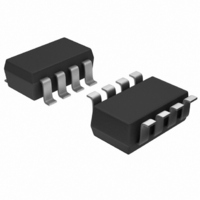
IC SW BUS CTRL 2.5/3.3V SOT23-8

ADG3243BRJ-R2

Manufacturer Part Number
ADG3243BRJ-R2
Description
IC SW BUS CTRL 2.5/3.3V SOT23-8
Manufacturer
Analog Devices Inc
Type
Bus Switchr
Datasheet

Specifications of ADG3243BRJ-R2

Rohs Status
RoHS non-compliant
Circuit
1 x 1:1
Independent Circuits
2
Voltage Supply Source
Single Supply
Voltage - Supply
2.5V, 3.3V
Mounting Type
Surface Mount
Package / Case
SOT-23-8
Operating Temperature
-
Current - Output High, Low
-
Other names
ADG3243BRJ-R2
ADG3243BRJ-R2TR
GENERAL DESCRIPTION
The ADG3243 is a 2.5 V or 3.3 V, 2-bit, 2-port digital switch
with individual channel control. It is designed on a low voltage
CMOS process, which provides low power dissipation yet gives
high switching speed and very low on resistance. This allows the
inputs to be connected to the outputs without additional propa-
gation delay or generating additional ground bounce noise.
The switches are enabled by means of the bus enable (BEx) input
signal. This digital switch allows a bidirectional signal to be
switched when ON. In the OFF condition, signal levels up to
the supplies are blocked.
This device is ideal for applications requiring level translation.
When operated from a 3.3 V supply, level translation from 3.3 V
inputs to 2.5 V outputs is allowed. Similarly, if the device is
operated from a 2.5 V supply and 2.5 V inputs are applied, the
device will translate the outputs to 1.8 V. This makes the device
suited to applications requiring level translation between different
supplies, such as converter to DSP/microcontroller interfacing.
REV. 0
Information furnished by Analog Devices is believed to be accurate and
reliable. However, no responsibility is assumed by Analog Devices for its
use, nor for any infringements of patents or other rights of third parties that
may result from its use. No license is granted by implication or otherwise
under any patent or patent rights of Analog Devices. Trademarks and
registered trademarks are the property of their respective companies.
FEATURES
225 ps Propagation Delay through the Switch
4.5
Data Rate 1.5 Gbps
2.5 V/3.3 V Supply Operation
Level Translation
Small Signal Bandwidth 710 MHz
8-Lead SOT-23 Package
APPLICATIONS
3.3 V to 2.5 V Voltage Translation
2.5 V to 1.8 V Voltage Translation
Bus Switching
Bus Isolation
Hot Swap
Hot Plug
Analog Switch Applications
3.3 V to 2.5 V
2.5 V to 1.8 V
Switch Connection between Ports
2.5 V/3.3 V, 2-Bit, Individual Control
PRODUCT HIGHLIGHTS
1. 3.3 V or 2.5 V supply operation.
2. Extremely low propagation delay through switch.
3. 4.5 Ω switches connect inputs to outputs.
4. Level/voltage translation.
5. Tiny SOT-23 package.
One Technology Way, P.O. Box 9106, Norwood, MA 02062-9106, U.S.A.
Tel: 781/329-4700
Fax: 781/326-8703
BE0
BE1
A0
A1
Level Translator Bus Switch
FUNCTIONAL BLOCK DIAGRAM
© 2003 Analog Devices, Inc. All rights reserved.
ADG3243
www.analog.com
B0
B1

Related parts for ADG3243BRJ-R2

ADG3243BRJ-R2 Summary of contents

Page 1

FEATURES 225 ps Propagation Delay through the Switch 4.5 Switch Connection between Ports Data Rate 1.5 Gbps 2.5 V/3.3 V Supply Operation Level Translation 3 2 1.8 V Small Signal Bandwidth 710 MHz 8-Lead ...

Page 2

ADG3243–SPECIFICATIONS Parameter DC ELECTRICAL CHARACTERISTICS Input High Voltage Input Low Voltage Input Leakage Current OFF State Leakage Current ON State Leakage Current Maximum Pass Voltage 3 CAPACITANCE A Port Off Capacitance B Port Off Capacitance A, B Port On Capacitance ...

Page 3

... Exposure to absolute maximum rating conditions for extended periods may affect device reliability. Only one absolute maximum rating may be applied at any one time. Model Temperature Range ADG3243BRJ-R2 –40°C to +85°C ADG3243BRJ-REEL –40°C to +85°C ADG3243BRJ-REEL7 – ...

Page 4

ADG3243 V Positive Power Supply Voltage. CC GND Ground (0 V) Reference. V Minimum Input Voltage for Logic 1. INH V Maximum Input Voltage for Logic 0. INL I Input Leakage Current at the Control Inputs OFF State ...

Page 5

3. 3. 0.5 1.0 1.5 2.0 2.5 3.0 3 ...

Page 6

ADG3243 –0.2 ON OFF C = InF L –0.4 –0 2.5V –0.8 CC –1.0 –1.2 –1.4 –1 3.3V CC –1.8 –2.0 0 0.5 1.0 1.5 2.0 2.5 3 ...

Page 7

TIMING MEASUREMENT INFORMATION For the following load circuit and waveforms, the notation that is used is V and V where IN OUT = = = V V and OUT ...

Page 8

ADG3243 BUS SWITCH APPLICATIONS Mixed Voltage Operation, Level Translation Bus switches can provide an ideal solution for interfacing between mixed voltage systems. The ADG3243 is suitable for applica- tions where voltage translation from 3.3 V technology to a lower voltage ...

Page 9

PLUG-IN CARD (1) CPU RAM PLUG-IN CARD (2) BUS Figure 10. ADG3243 in a Hot Plug Application There are many systems, such as docking stations, PCI boards for servers, and line cards for telecommunications switches, that require the ability to ...

Page 10

ADG3243 1.60 BSC 1.30 1.15 0.90 0.15 MAX OUTLINE DIMENSIONS 8-Lead Small Outline Transistor Package [SOT-23] (RJ-8) Dimensions shown in millimeters 2.90 BSC 2.80 BSC PIN 1 0.65 BSC 1.95 BSC 1.45 ...

Page 11

–11– ...

Page 12

–12– ...

Related keywords